To simulate return path PCB design using Ansys SIwave, you must first understand how return currents behave at high frequencies. This guide provides a step-by-step workflow for identifying and optimizing return paths in high-speed PCBs, ensuring signal integrity and reducing EMI.
Return Path Fundamentals for High-Speed PCB Design
In return path PCB design, the return current follows the path of least inductance at high frequencies, not least resistance. This path lies directly under the signal trace to minimize loop area. Key concepts include loop inductance, reference plane discontinuities (gaps or splits), and via stitching. A compromised return path can cause 20% eye closure at 10 Gbps.
Why Use Ansys SIwave for Return Path Simulation?
Ansys SIwave is the industry-standard tool for simulating return path PCB design due to its 3D EM solver (FEM and MoM), dedicated return path visualization, and integration with HFSS. It is trusted by Intel, Cisco, and Huawei for pre-layout and post-layout verification.
Step-by-Step Workflow: Simulate Return Path PCB Design Using Ansys SIwave
Step 1: Setting Up the PCB Model
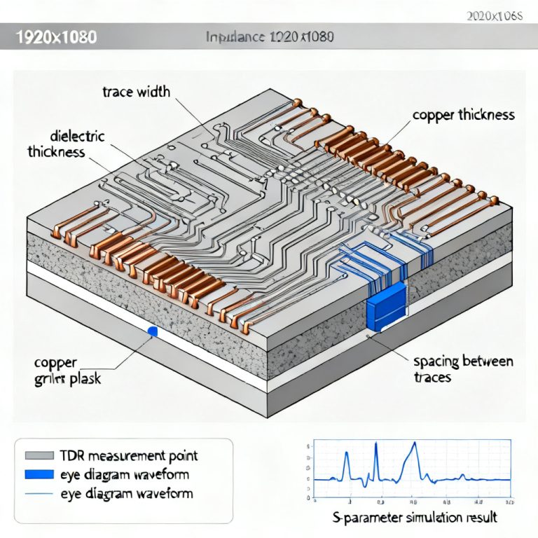
Import your PCB layout (ODB++, IPC-2581, Altium, Cadence). Verify stackup data (Dk, copper thickness). Assign ground and power planes as reference planes. Set frequency range (DC to 20 GHz). Mesh adaptively, refining around vias and gaps.
Step 2: Defining Ports and Excitation
Use lumped or wave ports at driver and receiver. Match port impedance to target (e.g., 50 ohms). Choose current source excitation for return path analysis. Specify signal amplitude and rise time.
Step 3: Running the Simulation
Select “Return Path Analysis” from the Simulate menu. Use “Net Group” for multiple nets. Monitor convergence (residual error below 1e-3).
Step 4: Analyzing Results
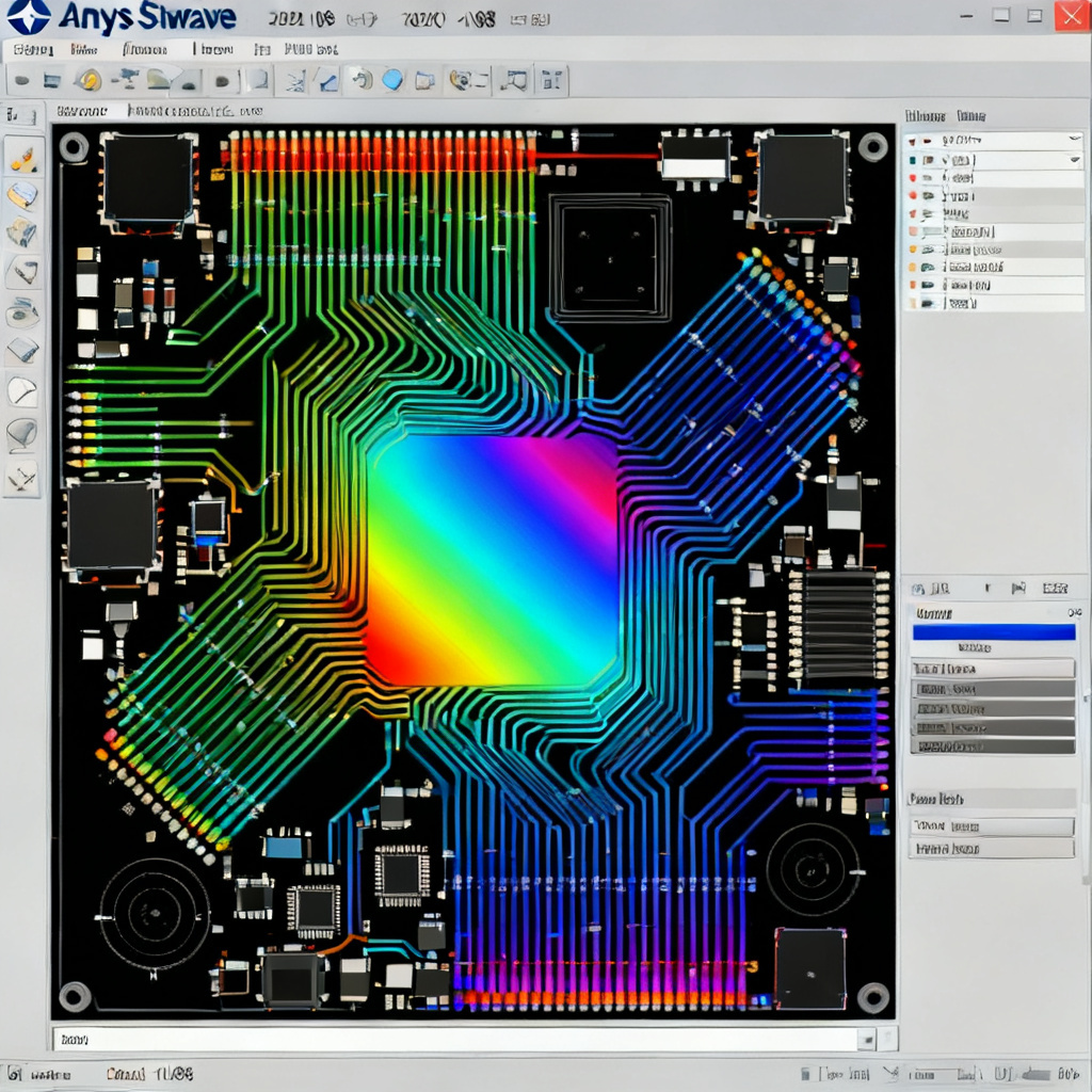
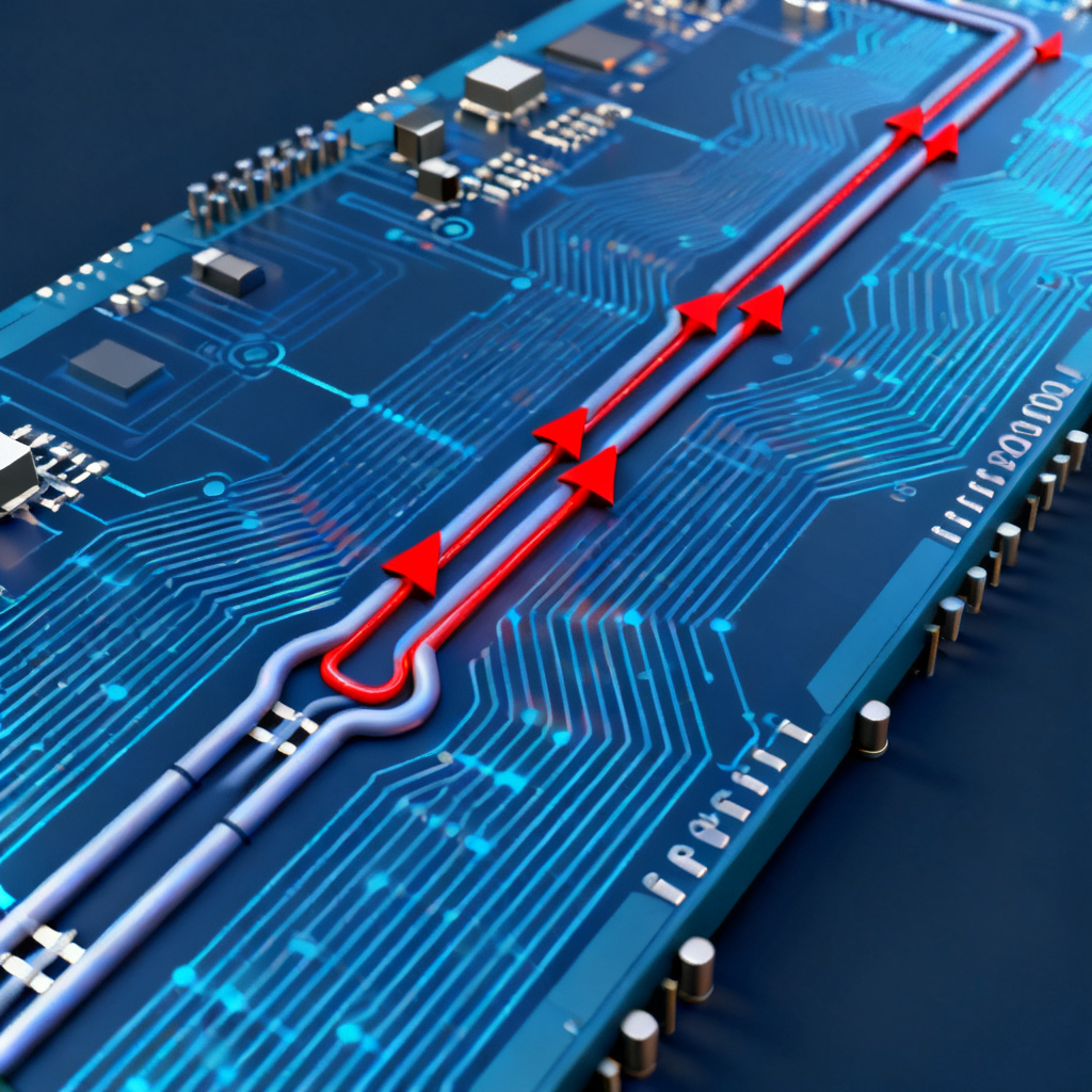
Visualize current density plots. High density under the trace indicates good return path. Identify gaps or slots causing discontinuities. Check loop inductance (target below 1 nH/inch for >5 Gbps). Compare S-parameters for insertion loss dips.
Advanced Techniques for Return Path Optimization
Run frequency sweeps to see low vs. high frequency return current behavior. For differential pairs, simulate odd-mode and even-mode return paths. Use stitching via optimization to reduce loop inductance. Predict EMI using far-field analysis.
Common Pitfalls in Return Path Simulation
| Pitfall | Consequence | Solution |
|---|---|---|
| Ignoring reference plane splits | Large loop area, increased EMI | Stitch planes with vias near signal transitions |
| Incorrect stackup data | Inaccurate inductance values | Verify Dk and thickness from manufacturer |
| Missing decoupling capacitors | Power plane impedance too high | Add decap models with ESL/ESR |
| Single-frequency simulation | Missed resonances | Run frequency sweep to 3x signal bandwidth |
| Overlooking via antipad size | Capacitive coupling, impedance mismatch | Adjust antipad for 50-ohm impedance |
Real-World Example: PCIe Gen 4 Return Path Optimization
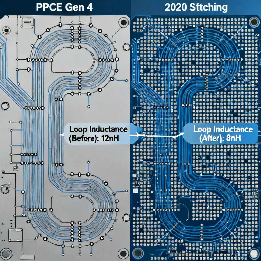
A 16-layer board with a 10 Gbps differential pair (PCIe Gen 4) was simulated. A split in the VDD plane caused loop inductance of 2.3 nH. After adding two stitching vias, loop inductance dropped to 0.8 nH, and insertion loss improved from -3 dB to -1.2 dB at 5 GHz.
FAQ: Return Path PCB Design Using Ansys SIwave
What is the return path in PCB design?
How does Ansys SIwave simulate return paths?
Why is return path simulation important for high-speed PCBs?
Why Choose Us for High-Speed PCB Manufacturing?
Our capabilities include controlled impedance (up to 10% tolerance), multilayer boards (up to 40 layers), and advanced materials (Rogers, Isola, Megtron). We support full SI/PI simulation with Ansys SIwave, ensuring your return path PCB design is optimized before fabrication.