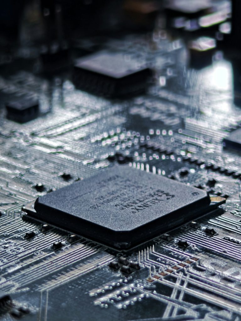
AI server PCB design has become the core hardware foundation for large AI model training, cloud data center clusters and multi-GPU parallel computing. Different from traditional standard server PCBs, AI server hardware relies heavily on OCP Accelerator Module (OAM), Universal Base Board (UBB) and GPU carrier boards, facing three major design challenges: ultra-high-speed PCIe 5.0/6.0 signal transmission, thousands of ampere high-current power delivery, and high-density compact layout with strict thermal limits.
This all-in-one pillar guide integrates OCP official industry standards, top PCB manufacturer mass-production experience and Megtron 6/8 professional material specifications. It systematically explains PCB classification, standard design parameters, high-speed routing rules, impedance control, power integrity, thermal management, material selection and practical design checklist. The content is professional enough for hardware engineers and PCB buyers, while keeping easy to understand for project decision-makers.
Overview of AI Server PCB Design
With the rapid expansion of artificial intelligence, large language models and generative AI applications, the global demand for high-performance AI servers continues to surge, bringing unprecedented high requirements for AI server PCB design. As detailed in the high speed PCB applications master page, AI servers represent one of the most demanding application scenarios for high-speed PCBs.
Traditional server PCBs cannot meet the demands of multi-GPU cluster interconnection, ultra-high-speed serial signal transmission and super high-current power supply. Modern AI server hardware is mainly composed of three core components: OAM accelerator modules, UBB universal base boards and GPU carrier boards. Each undertakes independent computing, interconnection and power distribution tasks.
The whole AI server PCB design process must overcome three core difficulties at the same time: support PCIe 5.0 and PCIe 6.0 high-speed differential signal transmission; bear thousands of amperes instantaneous high current under full load; balance high-density layout, signal integrity, power integrity and heat dissipation reliability. All design rules in this guide follow OCP Open Compute Project official specifications and international high-end PCB mass-production standards.
AI Server PCB Types: OAM, UBB and Switch Board
Each type of AI server PCB has clear functional positioning, layer standard and application scenario, forming the complete hardware topology of data center AI clusters. Understanding these types is essential for effective AI server PCB design.
。UBB
| PCB Type | Full Name | Core Function | Typical Layer Count |
|---|---|---|---|
| Universal Base Board | System main backplane, GPU & OAM interconnection, power distribution | 20–28 Layers | |
| OAM | OCP Accelerator Module | Pluggable AI acceleration unit, local high-density computing | 12–18 Layers |
| Switch Board | High-Speed Switch Board | Multi-node high-speed data exchange, expand SerDes bandwidth | 16–24 Layers |
UBB acts as the backbone of the entire AI server. It needs to arrange a large number of power layers and ground layers, so it adopts high-layer stackup to isolate crosstalk and stabilize power supply. OAM focuses on high-density BGA packaging routing, adopting medium layer count to balance performance, cost and heat dissipation. The switch board is optimized for high-speed channel layout, requiring complete ground shielding to reduce high-frequency interference.
Key Standard Design Parameters for OAM & UBB
Standardized parameters are the basis for unified AI server PCB design, purchasing specification and stable mass production. The following specifications comply with OCP standards and international high-end AI server PCB manufacturing norms.
| Parameter | UBB Specification | OAM Specification |
|---|---|---|
| Layer Count | 20–28 layers | 12–18 layers |
| Board Thickness | 2.5–4.0 mm | 2.0–3.2 mm |
| Min Line Width / Spacing | 4/4 mil | 3/3 mil / 2/2 mil |
| Main Material | Megtron 6 / Megtron 8 | Megtron 6 / Megtron 8 |
| Copper Thickness | 1–2 oz | 1–2 oz |
| Surface Treatment | ENIG | ENIG |
UBB uses relatively loose line width to reduce manufacturing difficulty and improve yield. OAM adopts ultra-fine 2/2mil and 3/3mil lines to adapt to high-density chip layout. ENIG is widely used for its excellent flatness, oxidation resistance and high-precision welding performance. Megtron 6 and Megtron 8 have become the standard substrate materials for high-end AI server PCB design, due to ultra-low high-frequency loss, high Tg value and excellent CAF resistance.
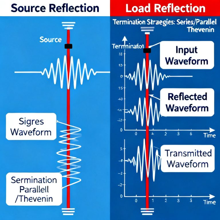
High-Speed Signal Routing & Impedance Control (PCIe 5.0/6.0)
High-speed signal integrity is the core of AI server PCB design, directly determining the stability and bandwidth of data interaction between OAM, UBB and GPU boards. For comprehensive PCIe layout rules, refer to PCIe PCB Design. For impedance formulas and tolerance guidelines, refer to Impedance Matching.
PCIe 5.0 and PCIe 6.0 differential pairs strictly require 100Ω differential impedance, with mass-production impedance tolerance controlled within ±10%. Excessive impedance deviation will cause signal reflection, jitter increase and higher bit error rate, even leading to link failure.
In daily routing design, engineers must follow these key rules for successful AI server PCB design:
- Control intra-pair length matching within 2–3mil to avoid timing skew
- Adopt tight coupling layout for high-speed differential pairs to reduce crosstalk — the foundational rules for Differential Pair Routing apply directly
- Minimize via quantity and avoid long stub resonance
- Use buried stripline routing as priority to enhance shielding effect
- Add ground stitching vias around high-speed channels to optimize return current path
These rules ensure stable transmission of 56Gbps and 112Gbps high-speed signals, fully matching the latest AI server interconnection standards.
High-Current Power Delivery Design
Multi-GPU and OAM parallel operation makes the peak current of a single AI server node reach thousands of amperes, which puts forward extremely strict requirements on PCB current carrying capacity and power integrity. This is a unique challenge in AI server PCB design not found in standard server boards.
- Adopt 3oz thick copper on outer layers and 2oz thick copper on inner power layers to reduce resistance and temperature rise
- Use multi-layer power plane overlapping layout to disperse current density
- Adopt via array design for high-current routes to avoid local overheating
- Conduct PDN voltage drop and current density simulation in the design stage
- Optimize component layout to shorten high-current transmission paths
Scientific high-current design can keep the working voltage of GPU and OAM chips within standard tolerance under full load, avoiding hardware throttling or automatic shutdown caused by insufficient power supply.
Material Selection & Thermal Management (Megtron 6/8)
PCB material performance directly affects high-frequency signal loss, high-temperature resistance, CAF reliability and overall heat dissipation effect. For detailed Dk/Df values of common laminates, refer to High-Speed PCB Material.
Core Material Requirements:
- Low signal loss: Megtron 6 and Megtron 8 feature ultra-low Dk/Df value, perfectly suitable for PCIe 5.0/6.0 and high-speed SerDes transmission
- High Tg performance: Glass transition temperature ≥170°C, adapting to long-term high-temperature working environment
- High CAF resistance: Effectively prevent electrochemical migration between vias and lines
- Stable dielectric performance: Maintain stable electrical parameters under high frequency and variable temperature
Thermal Management Solution: Adopt thick copper planes to enhance internal heat conduction; arrange dense thermal conduction vias under high-power chips; match external radiator structure; use symmetrical stackup design to reduce PCB warpage.
In practical selection, Megtron 6 is cost-effective for PCIe 5.0 and OAM short-range routing; Megtron 8 is preferred for PCIe 6.0 and UBB long-distance backplane interconnection. Material selection is a critical decision in AI server PCB design that directly affects signal integrity and cost.
AI Server PCB Design Checklist
Before design finalization and manufacturing release, follow this checklist to avoid design defects and production risks. This checklist ensures your AI server PCB design meets all critical requirements:
| ✅ | Item |
|---|---|
| ✅ | Complete length matching and skew calibration for all PCIe high-speed differential pairs |
| ✅ | Ensure all controlled impedance lines are within ±10% tolerance range |
| ✅ | Adopt symmetrical layer stackup to balance internal stress and prevent board warpage |
| ✅ | Verify copper thickness and line width of all high-current paths to meet peak load demand |
| ✅ | Optimize via-line spacing and select high CAF resistance materials |
| ✅ | Reduce stub length and apply back-drilling process for high-speed vias |
| ✅ | Check thermal via layout and heat dissipation design of high-power chip areas |
Key Takeaways for AI Server PCB Design
- AI server PCB design is mainly divided into UBB backplane, OAM accelerator module and high-speed switch board, each with fixed layer and parameter standards.
- Megtron 6/8 ultra-low-loss materials are the mainstream choice for PCIe 5.0/6.0 high-speed interconnection scenarios.
- Qualified AI server PCB design must balance high-speed signal integrity, thousands of ampere high-current power delivery and system thermal management.
- OCP official standards and DFM mass-production experience are essential references for engineers and purchasers.
- Symmetrical stackup, strict impedance control, reasonable copper thickness and CAF reliability design guarantee 24/7 stable operation of data center hardware.
FAQ About AI Server PCB Design
Q1: How many layers do OAM and UBB PCB usually use?
OAM adopts 12–18 layers; UBB universal base board uses 20–28 layers according to port quantity and power demand. This is a fundamental parameter in AI server PCB design.
Q2: Why use Megtron 6/8 instead of ordinary FR-4?
Regular FR-4 cannot control high-frequency signal loss under PCIe 5.0/6.0. Megtron 6/8 has lower dielectric loss, higher Tg and better CAF resistance, specially developed for AI high-speed server scenarios.
Q3: What is the standard impedance for PCIe 5.0/6.0 differential pairs?
Standard 100Ω differential impedance, production tolerance should be controlled within ±10%.
Q4: How to solve high-current overheating on AI server PCB?
Use 2–3oz thick copper, multi-layer power plane overlapping, via array layout and dense thermal vias, matched with radiator assembly design.
Q5: What is the best surface finish for OAM and UBB board?
ENIG is the most suitable option for flatness, oxidation resistance and high-precision BGA soldering.
Custom AI Server PCB Design & Manufacturing Inquiry
If you are developing OAM accelerator modules, UBB interconnection backplanes, GPU carrier boards or high-speed switch boards for AI servers, we provide one-stop professional support for your AI server PCB design needs: custom layer stackup & impedance simulation; PCIe 5.0/6.0 high-speed routing optimization; thick copper high-current PCB design; thermal management layout and DFM full verification; Megtron 6/8 ultra-low-loss material production.
Whether you need prototype sample production or mass supply for data center projects, send your design files, layer requirements and technical parameters to our team. We will arrange free technical review, customized solution and official quotation for you in the shortest time.
© 2026 HighSpeedPCBs