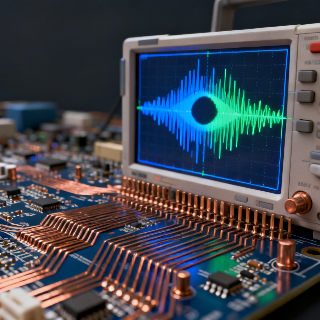
In high-speed PCB design, signal integrity (SI) is the difference between a working prototype and a field failure. The eye diagram—an oscilloscope display of a digital signal’s repetitive transitions—offers a single, powerful visualization of signal quality. For engineers designing PCBs for data rates above 1 Gbps, interpreting the eye diagram is non-negotiable. This pillar page dissects the three most critical eye diagram PCB parameters—Eye Height, Eye Width, and Eye Amplitude—explaining what each means, how they interact, and how they directly influence your PCB’s performance.
We draw from industry-leading sources, including Keysight Technologies, Teledyne LeCroy, and Texas Instruments, to provide a definitive guide. Whether you are specifying a high-speed backplane, a serializer/deserializer (SerDes) channel, or a DDR memory interface, understanding these parameters will elevate your design decisions.
Eye Amplitude: The Foundation of Signal Strength
What It Is
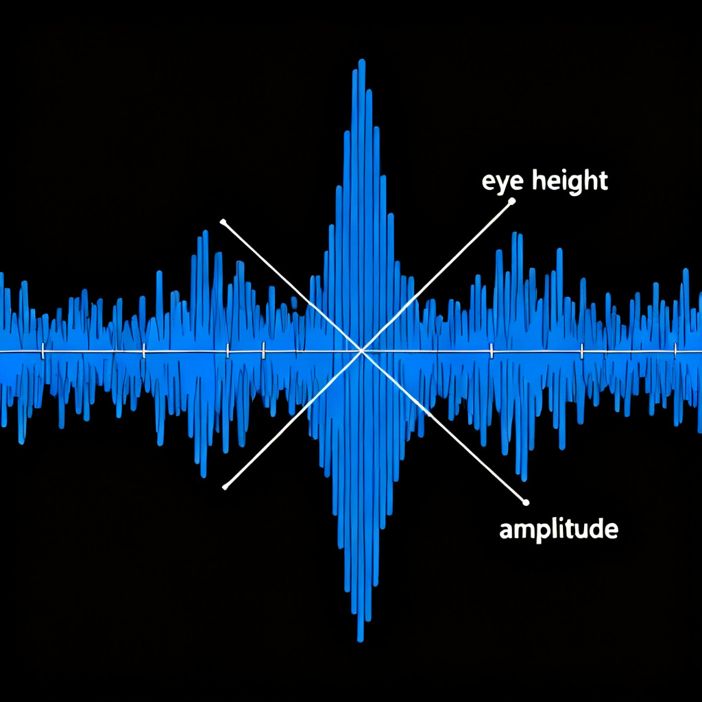
Eye amplitude is the absolute voltage difference between the logic high (1) and logic low (0) levels of a signal, measured at the center of the eye (the sampling point). It is the raw, undistorted voltage swing of the data signal, excluding noise and jitter.
How It’s Measured
- Vertical measurement: The difference between the mean voltage of the “1” level and the mean voltage of the “0” level.
- Key distinction: Unlike eye height, eye amplitude is measured before noise or jitter are considered. It represents the ideal, noise-free voltage swing.
- Typical unit: Millivolts (mV) or Volts (V).
Why It Matters for Your PCB
- Receiver Sensitivity: A larger eye amplitude provides a stronger signal for the receiver’s input stage. If the amplitude is too low, the receiver may fail to distinguish between logic levels, especially when driving long PCB traces or through multiple vias.
- Noise Margin: Higher amplitude directly increases the noise margin—the buffer between the signal and the receiver’s threshold. For high-speed PCBs, this margin is critical to withstand crosstalk from adjacent traces and power supply noise.
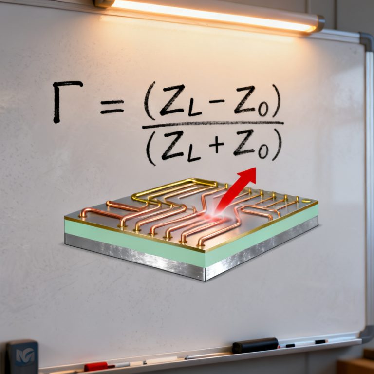
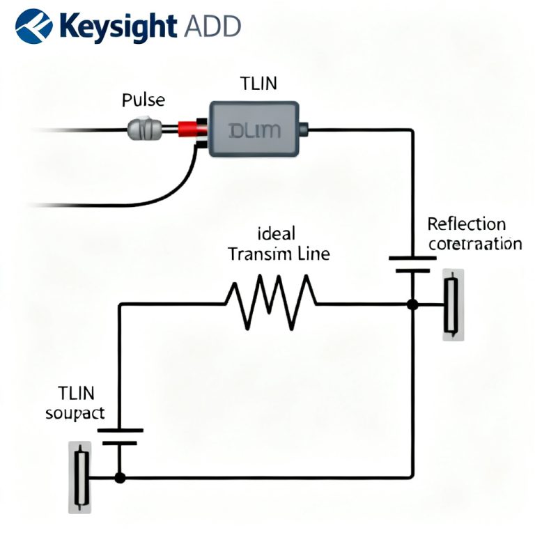
- Driver Capability: Amplitude is primarily set by the driver IC (e.g., a SerDes output) and the termination scheme. In PCB design, you can influence it via impedance matching. Mismatched termination (e.g., 50-ohm trace vs. 75-ohm termination) will reduce amplitude due to reflections.
Practical Example
A PCIe Gen 4 signal typically has an eye amplitude of 800 mV to 1.2 V. If your PCB’s trace impedance deviates from 85 ohms (differential), the amplitude may drop to 600 mV, risking receiver errors.
Eye Height: The Openness of the Eye
What It Is
Eye height is the vertical opening of the eye diagram at the center of the eye, measured from the bottom of the “1” level to the top of the “0” level, after noise and jitter have been accounted for. It is the actual usable voltage margin available to the receiver.
How It’s Measured
- Vertical measurement: The difference between the 5th percentile of the “1” level and the 95th percentile of the “0” level (or similar statistical thresholds, depending on the standard).
- Key distinction: Eye height is always less than eye amplitude because it subtracts noise (e.g., random jitter, crosstalk, power supply noise). It represents the worst-case signal swing at the sampling point.
- Typical unit: Millivolts (mV).
Why It Matters for Your PCB
- True Receiver Margin: While amplitude shows the ideal swing, eye height shows the real margin. A design with high amplitude but poor eye height (due to noise) will still fail.
- Impact of PCB Losses: Dielectric losses (e.g., FR-4 vs. low-loss materials) and conductor losses (skin effect) reduce eye height at higher frequencies. For a 10 Gbps signal on FR-4 over 20 inches, eye height may collapse to near zero.
- Crosstalk and EMI: Poor stackup design (e.g., insufficient spacing between layers) or lack of shielding reduces eye height. This is a key metric to optimize in your PCB layout.
Practical Example
Consider a USB 3.0 signal. The specification requires an eye height of at least 100 mV at the receiver. If your PCB has excessive via stubs or impedance discontinuities, the eye height may drop to 80 mV, causing link training failures.
Relationship with Eye Amplitude
- Eye Height = Eye Amplitude – Total Noise (Vertical).
- A healthy eye diagram should have eye height at least 50-70% of eye amplitude. If this ratio drops below 30%, your PCB has severe signal integrity issues.
Eye Width: The Time Margin for Data Capture
What It Is
Eye width is the horizontal opening of the eye diagram at the center of the eye, measured at a specific voltage threshold (typically 0 V for differential signals). It represents the time interval during which the receiver can reliably sample the data without errors.
How It’s Measured
- Horizontal measurement: The difference between the left and right crossing points of the eye at the zero-voltage level.
- Key distinction: Eye width is always less than the unit interval (UI) of the data rate. For example, a 10 Gbps signal has a UI of 100 ps. If the eye width is 60 ps, the remaining 40 ps is consumed by jitter.
- Typical unit: Picoseconds (ps) or as a percentage of UI.
Why It Matters for Your PCB
- Jitter Tolerance: Eye width directly measures the time margin available for the receiver’s clock recovery circuit. Low eye width means the receiver must sample near the edge of the data eye, increasing bit error rate (BER).
- Impact of PCB Impedance: Impedance mismatches (e.g., from connectors, vias, or stubs) cause reflections that shift the signal’s zero-crossing points, reducing eye width.
- Data Rate Limitation: As data rate increases, the UI shrinks. A 25 Gbps signal has a UI of 40 ps; if your PCB introduces 15 ps of jitter, the eye width drops to 25 ps, leaving almost no margin.
Practical Example
An Ethernet 10GBASE-KR backplane specification requires an eye width of at least 0.3 UI (e.g., 30 ps for 10 Gbps). If your PCB’s via stub length is 20 mils, it can add 5-10 ps of deterministic jitter, reducing eye width below the threshold.
Relationship with Eye Height
- These parameters are inversely correlated in many cases. Increasing eye height by boosting driver amplitude can sometimes increase jitter due to nonlinear effects, reducing eye width.
- The ideal design balances both: a large, open eye in both dimensions.
How These Parameters Interact in High-Speed PCB Design
Understanding the interplay between eye height, eye width, and eye amplitude is essential for optimizing your PCB.
- Amplitude vs. Height: A strong driver (high amplitude) is useless if the PCB introduces noise that collapses eye height. For example, a power supply with 50 mV ripple can reduce eye height by 30%.
- Width vs. Height Trade-off: In some designs, increasing pre-emphasis or de-emphasis (to boost high-frequency content) can improve eye height but may introduce overshoot that reduces eye width.
- The Eye Mask: Most high-speed standards (e.g., PCIe, USB, HDMI) define a “mask” in the eye diagram—a forbidden region at the center. The eye height and width must be large enough to keep the signal outside this mask. A violation at the mask’s corners indicates insufficient margin.
Key PCB Factors Affecting All Three
| Eye Diagram PCB Parameter | Key PCB Factor | Impact Description |
|---|---|---|
| Eye Amplitude | Impedance Matching | Mismatched termination reduces amplitude due to reflections. |
| Eye Height | Dielectric Material | Low-loss materials (e.g., Rogers, Megtron) preserve height at high frequencies. |
| Eye Width | Via Design | Minimize stub length; back-drilled vias reduce reflections that shrink width. |
| All Three | Power Integrity | Clean power planes reduce noise, improving height and width. |
Practical Measurement and Simulation Tips
To ensure your PCB meets eye diagram specifications, follow these best practices.
Simulation Before Fabrication
- Use tools like Keysight ADS, Ansys HFSS, or Cadence Sigrity to simulate the channel.
- Focus on the bathtub curve (BER vs. sampling point) to predict eye width and height at a target BER (e.g., 1e-12).
- Run statistical simulations to account for random jitter and noise.
Measurement on Prototypes
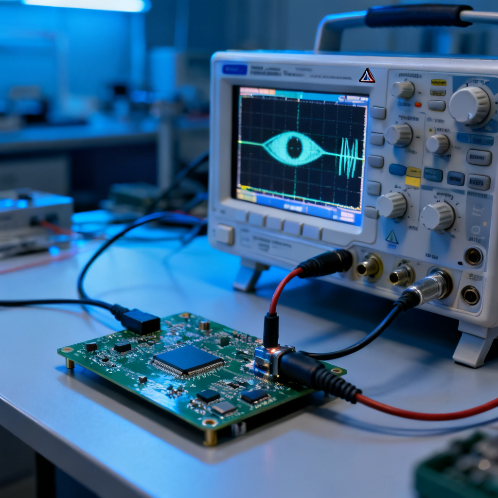
- Use a real-time oscilloscope with sufficient bandwidth (at least 3x the data rate).
- Capture at least 1 million UI to build a statistically valid eye diagram.
- Measure eye height at the mask (the central region) and eye width at the zero-crossing.
- Compare results to the standard’s mask compliance.
Common Pitfalls to Avoid
- Incorrect Triggering: Ensure the oscilloscope is triggered on the data clock, not the data itself.
- Short Acquisition Time: A 1000-UI eye may look perfect, but a 1-million-UI eye reveals jitter and noise.
- Ignoring Temperature: Eye parameters degrade with temperature. Test at the maximum operating temperature.
Case Study: Optimizing a 25 Gbps SerDes Channel
To illustrate, consider a 25 Gbps SerDes channel on a 12-layer PCB.
- Initial Design: FR-4 material, 8-inch trace, two vias with 30-mil stubs.
- Measured Eye Parameters:
- Eye Amplitude: 800 mV (good)
- Eye Height: 150 mV (marginal)
- Eye Width: 25 ps (poor; UI = 40 ps)
- Root Cause: Via stubs create reflections, reducing eye width. FR-4 losses reduce eye height.
- Optimization:
- Switch to Megtron 6 material (lower dielectric loss).
- Back-drill vias to reduce stub length to 5 mils.
- Add pre-emphasis (3 dB) at the driver.
- Result:
- Eye Height: 350 mV (improved by 133%)
- Eye Width: 32 ps (improved by 28%)
- Mask compliant at 1e-12 BER.
This demonstrates how understanding these parameters guides targeted PCB improvements.
Conclusion: Your High-Speed PCB Partner
Eye height, eye width, and eye amplitude are not abstract concepts—they are the measurable, actionable metrics that define your PCB’s signal integrity. By mastering them, you can:
- Specify appropriate materials and stackups.
- Design impedance-controlled traces and optimized vias.
- Validate performance through simulation and measurement.
At [Your Company Name], we specialize in manufacturing high-speed PCBs that meet the most stringent eye diagram requirements. From 1 Gbps to 112 Gbps PAM-4, our engineering team ensures your designs achieve the open eyes you need.
Ready to optimize your next high-speed PCB? [Contact us for a free signal integrity review] or [Download our high-speed design guide].
Frequently Asked Questions (FAQ)
What is the difference between eye height and eye amplitude in eye diagram PCB parameters?
Eye amplitude is the raw voltage swing between logic levels, while eye height is the usable voltage margin after subtracting noise. Both are critical eye diagram PCB parameters for assessing signal integrity.
How does eye width affect high-speed PCB performance?
Eye width determines the time margin for data sampling. A narrow eye width increases bit error rates, making it a key eye diagram PCB parameter for high-speed serial links.
Can eye diagram PCB parameters be improved through PCB design?
Yes, optimizing impedance control, using low-loss materials, and minimizing via stubs can significantly improve eye height, eye width, and eye amplitude in your PCB.