Article Summary
Jitter issues pcb are the top hidden threat to signal integrity in high-speed PCB and digital communication systems. Jitter issues pcb occur when clock and data signal edges deviate from their ideal timing position, resulting in narrowed eye diagrams, reduced timing margin, rising bit error rate, unstable data links and intermittent system crashes. This ultimate pillar guide to jitter issues pcb integrates professional technology from Tektronix, Cadence and industry PCB design resources, explaining jitter classification, visible symptoms, root causes, professional measurement methods, targeted fixes, standard troubleshooting workflow and design prevention checklists.
1. Jitter – When Signal Edges Lose Ideal Timing Position
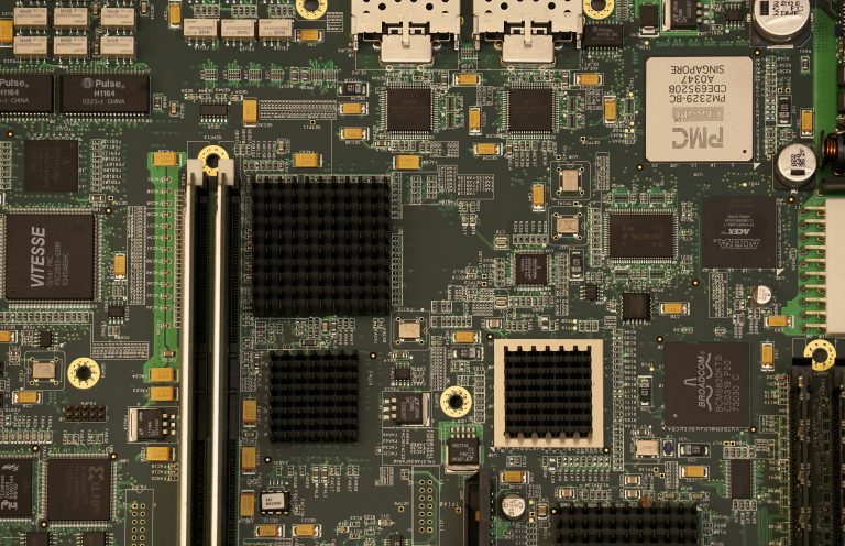
In high-speed PCB design, stable timing alignment of clock and data edges is the core guarantee of system reliability. Jitter is defined as the unwanted deviation of signal rising and falling edges from their ideal periodic timing position on transmission lines. As detailed in the High-speed PCB troubleshooting master page, jitter issues pcb are among the most critical signal integrity failures.
With the continuous improvement of data rate, the unit interval of bit signal is compressed to picosecond level. Even tiny jitter issues pcb will directly shrink the eye opening width and significantly increase BER (Bit Error Rate). It further leads to link training failure, data loss, intermittent restart and other difficult-to-reproduce faults in high-speed interfaces such as PCIe, Ethernet, USB4 and DDR.
In industry standard classification, jitter is divided into two core categories:
- Random Jitter (RJ): Unbounded Gaussian distribution noise, originated from intrinsic device noise
- Deterministic Jitter (DJ): Bounded and predictable timing deviation, caused by PCB design, layout and power integrity defects
Mastering the classification and mechanism of jitter is the first step to solve jitter issues pcb fundamentally, rather than relying on blind debugging.
2. Clear Symptoms of Serious PCB Jitter Problems
Jitter issues pcb will produce obvious measurable symptoms in the early stage. Engineers can quickly judge the severity through oscilloscope eye diagram test and link stability detection. Early identification can avoid mass production yield loss and after-sales failure.
| Symptom | Measurement Performance | Severity Level |
|---|---|---|
| Narrow Eye Width | Timing margin shortage, horizontal eye diagram compression | High |
| Rising Bit Error Rate | BER exceeds specification standard, sporadic data corruption | High |
| Unstable Data Link | Frequent link retraining, handshake failure, intermittent disconnection | High |
| Eye Diagram Overlap | Serious horizontal closure, signal edge aliasing | Extremely High |
Low-amplitude jitter only causes marginal timing loss; excessive jitter issues pcb will directly collapse the eye diagram, resulting in unable to sample data normally. Most jitter faults are intermittent, only appearing under temperature drift, load surge and full-speed operation, so eye diagram comparison is the most intuitive diagnosis method. For related issues, see PCB crosstalk issues.
3. Jitter Types, Features and Fundamental Root Causes
Total Jitter (TJ) is superposed by RJ and DJ. Deterministic jitter can be further subdivided into multiple types. Understanding these types is essential for diagnosing jitter issues pcb. For PCB reflection issues, similar impedance-related analysis applies.
| Type | Abbreviation | Core Feature | Root Causes |
|---|---|---|---|
| Random Jitter | RJ | Unbounded Gaussian, unpredictable | Thermal noise, shot noise, semiconductor intrinsic noise |
| Deterministic Jitter | DJ | Bounded non-Gaussian, repeatable error | Impedance discontinuity, layout defect, power noise |
| Data-Dependent Jitter | DDJ | Timing offset related to data code pattern | Insufficient bandwidth, transmission line reflection, ISI |
| Duty Cycle Distortion | DCD | Asymmetric pulse width, inconsistent edge speed | Driver rise/fall mismatch, unbalanced differential pair |
| Periodic Jitter | PJ | Regular periodic timing fluctuation | Power supply ripple, switching regulator noise |
| Crosstalk Jitter | — | Timing distortion induced by adjacent traces | Too small spacing, long parallel routing, unshielded aggressor |
Random jitter cannot be completely eliminated, only reduced by optimizing the system noise floor. All deterministic jitter is caused by man-made design and layout problems, which can be completely solved through impedance optimization, power filtering and layout adjustment.
Power ripple and crosstalk are the two most common jitter issues pcb sources in industrial and consumer high-speed PCBs.
4. Jitter Measurement and Decomposition Professional Methods
Accurate jitter troubleshooting must rely on professional test instruments to capture waveforms, separate jitter components and quantify the contribution ratio of RJ and DJ. Solving jitter issues pcb requires data decomposition. For PCB Manufacturing, proper testing protocols are essential for mass production verification.
| Test Tool | Main Application | Core Output |
|---|---|---|
| High-Speed Oscilloscope | Capture waveform, eye diagram and TIE timing error | Total jitter value, eye opening parameter |
| Jitter Analysis Software | Intelligent decomposition of total jitter | Separate RJ/DJ, bathtub curve, BER report |
| Spectrum Analyzer | Locate periodic interference frequency | PJ frequency peak, interference source positioning |
| VNA Vector Network Analyzer | Test impedance and phase noise | Impedance mismatch point, clock phase noise |
Eye diagram is the first quick inspection standard for judging jitter issues pcb severity. Jitter analysis software uses statistical algorithms to separate Gaussian random noise from bounded deterministic jitter. Spectrum analysis is especially suitable for finding periodic jitter caused by switching power supply. VNA can accurately locate reflection points that induce DDJ jitter.
5. Practical Solutions to Reduce and Fix PCB Jitter
Blind noise reduction has little effect. The most efficient way to resolve jitter issues pcb is to match the solution according to the jitter type. For High-Speed PCB Material, proper material selection also impacts jitter performance.
| Jitter Type | Optimization Solution | Improvement Effect |
|---|---|---|
| Random Jitter (RJ) | Select low-noise components, optimize grounding, reduce thermal noise | Moderate |
| Data-Dependent Jitter (DDJ) | Strict impedance matching, eliminate trace discontinuity, add termination | High |
| Duty Cycle Distortion (DCD) | Match driver edge slew rate, symmetrical differential routing | High |
| Periodic Jitter (PJ) | Suppress power ripple, add LDO, isolate switching noise | High |
| Crosstalk Jitter | Increase trace spacing, shorten parallel length, add ground shielding | High |
| Overall System Jitter | High-precision low-jitter clock, optimize signal and power integrity | Very High |
For PCB engineers, standardized impedance control, differential pair equal-length design and sufficient power decoupling are the most daily and effective means to suppress deterministic jitter.
Replacing low-quality clock sources can fundamentally reduce the overall baseline jitter caused by jitter issues pcb.
6. Step-by-Step Jitter Troubleshooting Flowchart
Follow this standardized process to avoid trial-and-error modification and quickly locate jitter issues pcb root cause:
Step 1: Use high-speed oscilloscope to capture eye diagram and TIE waveform, quantify total jitter severity.
Step 2: Decompose total jitter through professional software to separate RJ, DJ and each sub-jitter component.
Step 3: Confirm the dominant jitter type, judge whether it comes from device noise, layout crosstalk, power ripple or impedance reflection.
Step 4: Adopt targeted rectification: layout adjustment for crosstalk, power filtering for PJ, edge matching for DCD, low-noise device replacement for RJ.
Step 5: Re-test eye diagram, jitter value and BER index to verify whether it meets design specification.
This closed-loop workflow of measurement-decomposition-positioning-optimization-verification is essential for solving jitter issues pcb efficiently.
7. Jitter Prevention Checklist for PCB Design Stage
The most cost-effective way to control jitter issues pcb is to embed prevention rules in the initial design, rather than repairing problems after prototype production:
- Select industrial-grade low-jitter clock oscillator and high-stability PLL chip
- Design low-noise power rail, configure multi-value decoupling capacitors, isolate switching power circuit
- Strictly implement controlled impedance routing for all high-speed signal lines
- Keep differential pairs equal in length and symmetrical in routing to avoid timing skew
- Place decoupling capacitors close to IC power pins to ensure local power filtering
- Reasonably control trace spacing and limit parallel routing length to suppress crosstalk
- Maintain complete ground plane integrity to avoid reference plane discontinuity inducing reflection jitter
Implementing these rules can eliminate more than 80% of deterministic jitter issues pcb hidden dangers in advance.
8. Key Takeaways
- Jitter issues pcb are divided into random jitter (intrinsic noise) and deterministic jitter (design defect). RJ can only be reduced, while DJ can be completely eliminated by design optimization
- Excessive jitter has obvious measurable symptoms such as narrow eye width, excessive BER and unstable high-speed link
- Professional instruments and jitter decomposition software are necessary means to accurately locate jitter issues pcb root causes
- Clock quality and power integrity are the two most critical factors affecting system-level jitter performance
- Standardized troubleshooting process and early design prevention are far more efficient than later blind debugging
For a complete understanding of all troubleshooting topics, return to the High-speed PCB troubleshooting master page.
9. FAQ on PCB Jitter Issues
Q1: What are the main causes of jitter in high-speed PCB?
The main triggers are power supply ripple, trace crosstalk, impedance mismatch reflection and low-precision clock source. These are the most common jitter issues pcb sources.
Q2: What is the essential difference between RJ and DJ?
RJ is unbounded Gaussian thermal noise, which cannot be eliminated; DJ is bounded and predictable, caused by PCB layout, power supply and hardware mismatch, which can be completely fixed.
Q3: Can jitter be solved only by software configuration?
Software setting can only slightly relieve symptoms. Most jitter issues pcb need hardware layout optimization, power circuit improvement or component replacement to solve fundamentally.
Q4: How to quickly judge whether PCB has serious jitter?
Capture eye diagram through high-speed oscilloscope; obvious eye closure and edge overlap mean excessive jitter.
Q5: How does power ripple affect jitter?
Switching power supply ripple directly modulates clock and data edges. For solutions, see signal attenuation issues which covers power integrity impact on signal quality.
10. Professional Jitter Analysis & Custom Solution Inquiry
Jitter issues pcb troubleshooting and signal integrity optimization require rich engineering experience in high-speed layout, eye diagram interpretation, jitter decomposition and power integrity design.
If your project encounters intermittent data errors, eye diagram closure, BER over-standard, link instability and unknown timing jitter problems, our professional team can provide jitter root cause analysis, PCB design review, layout optimization guidance and targeted jitter suppression solution customization.
We serve global industrial electronic buyers, hardware engineers and manufacturers, providing one-stop technical support from design optimization to mass production stability.
📧 Contact us now for free technical consultation and project quotation – we will tailor the most reliable jitter solution according to your application scenario and specification requirements.