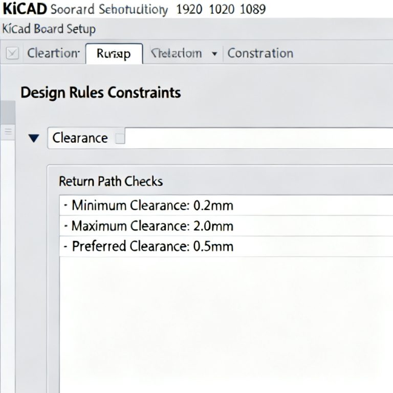
How to Set Up Return Path PCB Design Checks in Your EDA Tool Altium Cadence KiCad
In high-speed PCB design, the return path is not an afterthought—it is the foundation of signal integrity. A poorly designed return path creates ground loops, increases electromagnetic interference (EMI), and degrades signal quality. For B2B engineers designing high-speed PCBs for export, ensuring a continuous, low-impedance return path is critical. This Pillar Content provides a definitive…