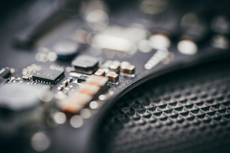
The Complete Workflow of High Speed PCB Design From Schematic to Fabrication
The complete High Speed PCB Design workflow from schematic to fabrication is a structured, iterative process that ensures signal integrity, power integrity, and manufacturability. This guide covers every critical step for reliable High Speed PCB performance. High Speed PCB Design Pre-Layout Planning The foundation of any successful High Speed PCB Design is a meticulously crafted…