5g telecom pcb design lays the fundamental hardware foundation for modern 5G network infrastructure deployment. It covers AAU, RU, DU and small cell infrastructure, dealing with mixed high-frequency RF and high-speed digital signals. As one important branch under industry PCB applications, this article walks through high-frequency material selection, hybrid stackup structure, passive intermodulation control, impedance tuning, thermal design and outdoor reliability standards. It is tailored for RF engineers, hardware designers and global procurement buyers in the telecom industry.
Table of Contents
- Overview of 5G Telecom PCB Design
- 5G Base Station PCB Types & Architecture
- High-Frequency Materials and Hybrid Stackup
- Passive Intermodulation (PIM) Control Core Rules
- AAU and RU Professional Design Guidelines
- DU and Small Cell PCB Design Requirements
- Environmental and Long-Term Reliability
- 5G Telecom PCB Design Checklist
- Key Takeaways
- FAQ
- Get Professional Design & Quotation Support
Overview of 5g telecom pcb design
5g telecom pcb design is one of the most technically demanding branches in high-frequency and high-speed circuit development. Modern 5G networks adopt a split architecture composed of AAU, RU and DU, working alongside compact small cell units to achieve wide-area and hotspot coverage.
With the evolution to millimeter-wave FR2 bands at 24–40GHz, traditional FR4-only PCB solutions can no longer meet the requirements of low insertion loss and stable dielectric performance. Unlike consumer electronics, telecom base station PCBs must maintain stable performance over decade-long outdoor operation under extreme temperature, humidity and vibration.
Many high-speed design principles used in 5G base station hardware are closely shared with data center PCB design, especially in stackup optimization, differential signal control and impedance consistency management.
5G Base Station PCB Types & Architecture
Each 5G functional unit has distinct layer counts, material requirements and application scenarios, forming the core classification basis for 5g telecom pcb design.
| Unit | Function | Typical Layers | Core Requirements |
|---|---|---|---|
| AAU | Antenna + RF front-end | 8–12 | High-frequency hybrid stackup, low loss, 50Ω impedance |
| RU | RF transceiver unit | 6–10 | Low PIM, stable Dk, weather resistance |
| DU | Baseband processing | 12–20 | Low-loss high-speed material, 100Ω differential |
| Small Cell | Miniature coverage base station | 6–8 | High density, compact layout, heat dissipation |
DU baseband boards adopt similar high-speed interconnection standards as AI server PCB design, requiring strict control over via stub, length matching and multi-layer power integrity.
High-Frequency Materials and Hybrid Stackup
Material selection determines the loss performance and service life of 5g telecom pcb design. The mainstream materials are divided into PTFE-based substrates and hydrocarbon ceramic laminates.
- PTFE series: RO3003, RO5880, ultra-low Df, suitable for millimeter-wave AAU RF layers
- Hydrocarbon series: RO4350B, RO4725, balanced cost and performance, widely used in RU radio units
- Hybrid stackup: Combine high-frequency material for RF layers and standard FR4 for digital layers
This hybrid solution is the most cost-effective mainstream choice for large-scale 5G commercial deployment.
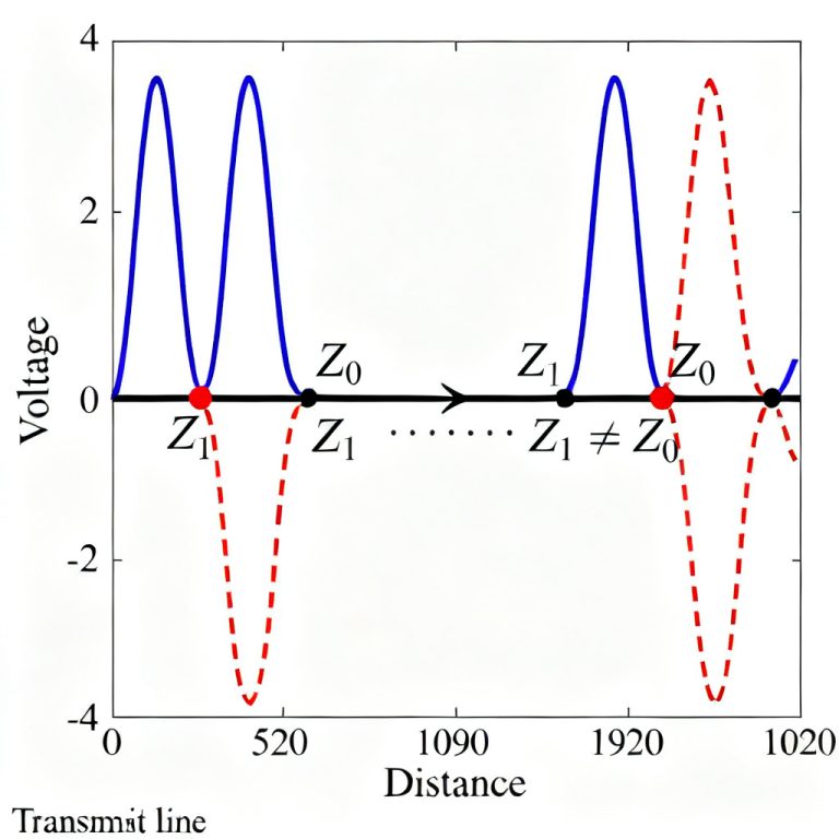
Passive Intermodulation (PIM) Control Core Rules
PIM is the biggest hidden risk in carrier-grade 5g telecom pcb design. Uncontrolled passive intermodulation will generate clutter interference, reduce receiver sensitivity and shrink actual coverage radius.
Key control methods:
- Adopt non-magnetic surface finishing to avoid magnetic loss
- Control copper foil roughness to reduce signal scattering loss
- Maintain complete reference ground plane for all RF traces
- Optimize via stitching and grounding density
- Avoid material oxidation and surface contamination during production
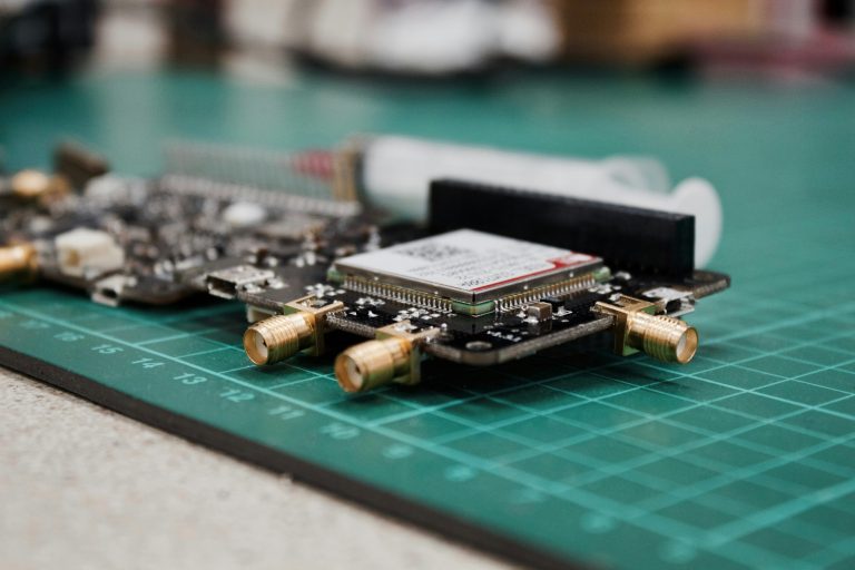
AAU and RU Professional Design Guidelines
AAU and RU are the core RF carriers of 5G networks, with fixed design specifications for 5g telecom pcb design:
- Strict 50Ω single-ended impedance for all RF lines
- Dk dielectric constant stability controlled within ±0.05
- High CAF-resistant material for long-term outdoor use
- 45° arc routing instead of right-angle turns
- Isolate high-power amplifier area from weak signal receiving area
DU and Small Cell PCB Design Requirements
DU focuses on 25G / 50G high-speed Ethernet and large-capacity data transmission. Its high-speed interface design follows the same precision standards as HDMI PCB design, emphasizing differential pair length matching, impedance tolerance and crosstalk suppression.
Small cell products pursue miniaturization and high integration, requiring compact layer structure, fine line width and optimized thermal via layout to solve heat accumulation in sealed equipment.
Environmental and Long-Term Reliability
5G telecom PCBs work in harsh outdoor environments for a long time, and reliability is a must in qualified 5g telecom pcb design.
- Operating temperature: -40°C ~ 85°C
- Salt spray resistance for coastal deployment
- Conformal coating for moisture and dust protection
- Thermal cycling and vibration mechanical reliability
- Lightning surge protection layout design
Only by meeting these reliability indicators can PCB design reach operator acceptance standards.
5G Telecom PCB Design Checklist
Before prototype and mass production, verify all key items for 5g telecom pcb design:
- High-frequency model selection matches millimeter-wave and Sub-6G scenarios
- Hybrid stackup structure and lamination stability confirmed
- Full PIM control measures implemented in layout and material
- 50Ω RF impedance and 100Ω differential strictly calibrated
- Thermal design optimized for high-power modules
- Outdoor environmental reliability indicators fully complied
Key Takeaways
5g telecom pcb design integrates RF material technology, high-speed signal integrity, PIM suppression and outdoor reliability engineering. AAU and RU rely on high-frequency low-loss substrates; DU borrows high-speed design experience from server and data center hardware; small cell balances miniaturization, heat dissipation and cost. Hybrid stackup remains the most practical solution for large-scale 5G projects.
FAQ
Q1: What are the most common materials for 5G telecom PCB?
A: RO4350B, RO3003 and RO5880 are the mainstream high-frequency materials, matched with FR4 to form hybrid stackup.
Q2: Why is PIM control so important for 5G base station PCB?
A: PIM interference seriously affects receiving sensitivity and network coverage, which is a must-pass test for carrier-grade equipment.
Q3: What impedance is used in 5G PCB design?
A: RF signal adopts 50Ω single-ended impedance; high-speed differential pairs use 100Ω standard.
Get Professional Design & Quotation Support
If you are developing AAU, RU, DU, small cell and other telecom PCB projects, we provide one-stop 5g telecom pcb design consulting, stackup design, impedance simulation and turnkey manufacturing service.
We also support customized development and production for automotive PCB design and optical module PCB guide high-frequency high-speed board projects.
Feel free to send your layer requirement, application frequency and project volume to us, and get a free DFM check, professional technical solution and official quotation.