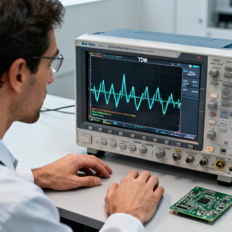
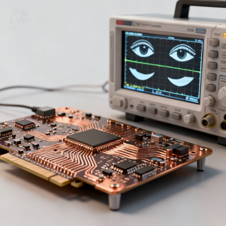
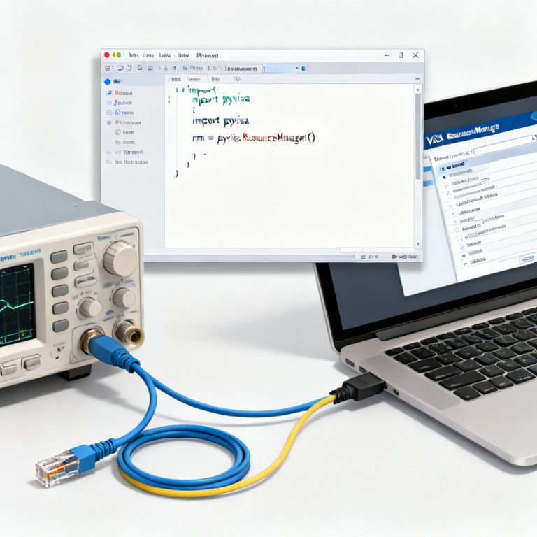
In high-speed PCB design, signal integrity (SI) is paramount. As data rates push beyond 10 Gbps, the margin for error shrinks to picoseconds. The most critical metric for evaluating signal quality is jitter decomposition in eye diagram PCB—the analysis of timing deviations into Random, Deterministic, and Total Jitter.
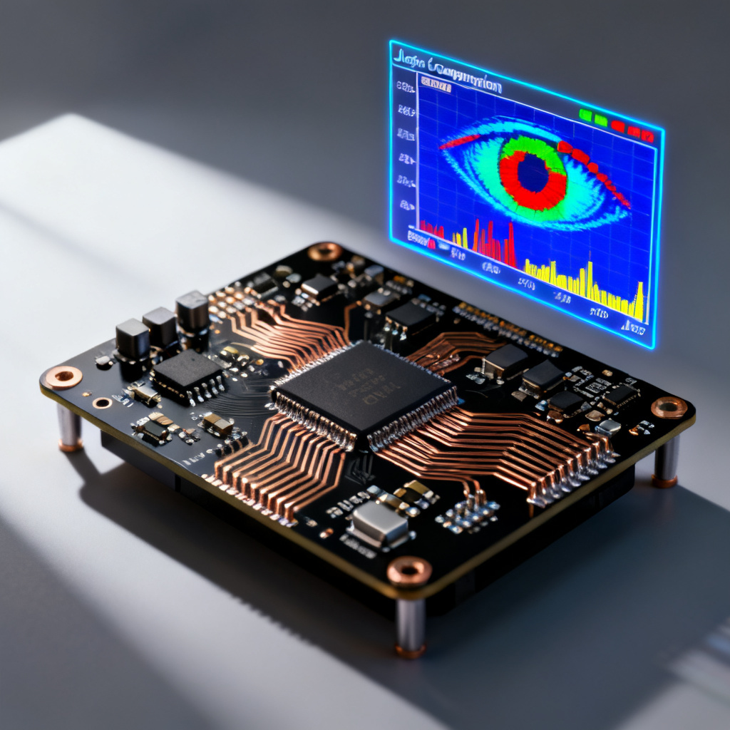
What is Jitter and Why Decompose It?
Jitter is defined as the short-term variation of a digital signal’s significant instants (e.g., rising or falling edges) from their ideal timing positions. In an eye diagram, jitter manifests as the horizontal “blurring” or thickening of the eye opening. A closed eye means bit errors; a wide-open eye means a reliable link.
Why decompose jitter?
- Diagnosis: Identifying the root cause of jitter (e.g., power supply noise vs. random thermal noise) dictates the fix.
- Compliance: Standards like PCIe Gen 5/6, USB 3.2, and 100G Ethernet require specific jitter budgets for RJ and DJ.
- Budgeting: Designers allocate jitter margins to different sub-systems (transmitter, channel, receiver). Without decomposition, you cannot know which part is failing.
Key Insight from Industry Leaders: Jitter decomposition is not just a measurement—it is a design methodology. A single jitter number (TJ) hides the underlying physics.
Total Jitter (TJ): The Big Picture
Total Jitter (TJ) is the peak-to-peak variation of a signal’s edges at a specified bit error rate (BER), typically 10-12 for high-speed serial links. TJ is not simply the sum of Random and Deterministic jitter—it is a statistical projection.
Formula (Dual-Dirac Model):
TJ(BER) = DJp-p + 2 × α × RJrms
Where:
- DJp-p = Peak-to-peak deterministic jitter (bounded)
- RJrms = Root-mean-square random jitter (unbounded, Gaussian)
- α = A constant derived from the BER (e.g., α = 7.44 for BER = 10-12)
Important Nuance from Top Sources:
- The Dual-Dirac model assumes that the jitter distribution has two Gaussian “Dirac” peaks (left and right edges). This is a simplification, but it is the industry standard for compliance.
- TJ at lower BER (e.g., 10-15) grows rapidly because RJ is unbounded. This is why RJ must be measured with extreme precision.
Practical PCB Implication:
A TJ of 0.3 UI (Unit Interval) at BER=10-12 is typical for a 10 Gbps link. If your eye diagram shows a TJ exceeding 0.5 UI, the link will likely fail. Decomposition tells you which component to attack.
Deterministic Jitter (DJ): The Predictable Enemy
Deterministic Jitter (DJ) is bounded, predictable, and non-Gaussian. It has a finite peak-to-peak amplitude and is caused by identifiable, repeatable sources. DJ is further broken down into sub-components.
Data-Dependent Jitter (DDJ)
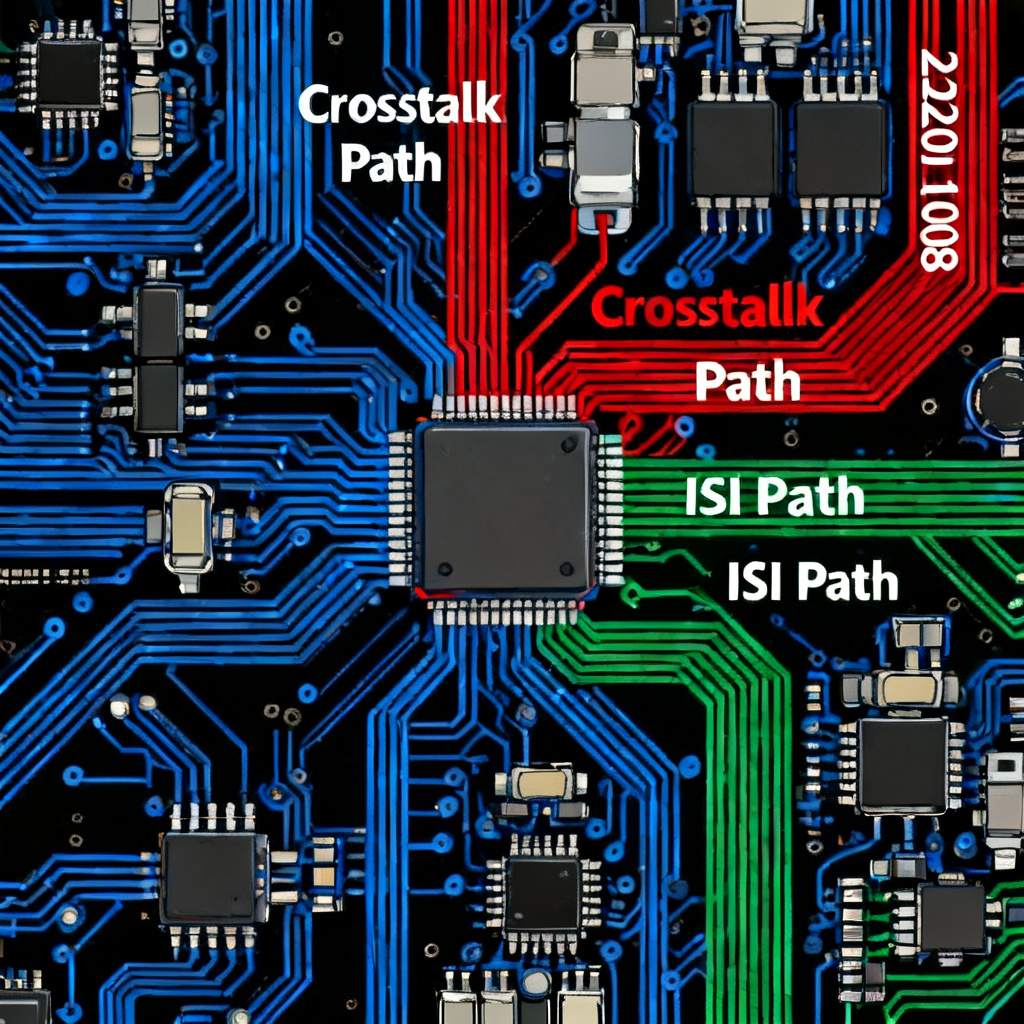
- Cause: Intersymbol Interference (ISI) due to channel bandwidth limitations (lossy dielectrics, impedance mismatches, stubs).
- Behavior: Jitter depends on the specific bit pattern (e.g., “1010” vs. “1111”).
- Measurement: DDJ is extracted by averaging the waveform over many repetitions of a known pattern (e.g., PRBS7 or PRBS15).
- PCB Fix: Reduce channel loss by using lower-loss laminates (e.g., Megtron 6 vs. FR-4), optimize via backdrilling, and minimize stub length.
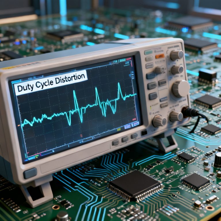
Duty Cycle Distortion (DCD)
- Cause: Asymmetry in the rising vs. falling edge propagation delays. Common sources: differential skew in the driver IC, unequal rise/fall times, or a threshold voltage offset in the receiver.
- Behavior: The eye diagram shows a systematic shift—the crossing point moves up or down.
- PCB Fix: Ensure matched trace lengths for differential pairs; avoid DC offsets in receiver termination.
Periodic Jitter (PJ)
- Cause: Coupling from periodic noise sources: power supply ripple (e.g., 60 Hz or switching regulator harmonics), clock feedthrough, or crosstalk from adjacent aggressor signals.
- Behavior: Sinusoidal modulation of the edge timing. In the frequency domain (phase noise plot), you see discrete spurs.
- PCB Fix: Improve power integrity (low-ESR decoupling caps, ferrite beads), isolate high-speed traces from clock lines, and use differential signaling to reject common-mode noise.
Bounded Uncorrelated Jitter (BUJ)
- Cause: Crosstalk from other high-speed signals that are not synchronous with the victim signal (e.g., an adjacent PCIe lane).
- Behavior: Appears as a random-looking but bounded jitter (not Gaussian).
- PCB Fix: Increase trace spacing, add ground vias as stitching, avoid parallel routing over long distances.
Expert Tip from Test Equipment Vendors:
To isolate DJ, use a bathtub curve (BER vs. sampling phase). The slope of the bathtub curve at low BER (the “tails”) is dominated by RJ, while the flat regions indicate DJ. A non-linear bathtub curve suggests complex DJ components.
Random Jitter (RJ): The Unavoidable Gaussian Noise
Random Jitter (RJ) is unbounded, Gaussian-distributed, and caused by fundamental physical processes:
- Thermal noise (Johnson-Nyquist) in resistors and transmission lines.
- Shot noise in semiconductor junctions.
- Flicker noise (1/f noise) in active devices (low-frequency phase noise).
Key Characteristics:
- RJ is quantified by its RMS value (σ), not peak-to-peak, because it has no theoretical limit.
- In the eye diagram, RJ appears as a gradual thickening of the edges, without a sharp boundary.
- RJ is uncorrelated with the data pattern or any periodic source.
Measurement Challenge:
- Because RJ is Gaussian, measuring it accurately requires a large number of samples (millions of bits) to resolve the tails.
- Common method: Phase noise analysis using a spectrum analyzer or a real-time oscilloscope with a high-resolution timebase.
PCB Design Mitigation (Limited but Critical):
- You cannot eliminate RJ, but you can minimize its impact:
- Use low-noise voltage regulators (LDOs) for PLL and clock circuits.
- Avoid excessive trace lengths (which increase thermal noise).
- Use differential signaling (common-mode rejection reduces noise coupling).
Important Distinction from Industry Sources:
RJ is often confused with BUJ (Bounded Uncorrelated Jitter). BUJ looks random but is actually bounded—it will not cause the infinite tails of a Gaussian distribution. Decomposition algorithms (e.g., tail-fitting) separate these by analyzing the histogram tails.
Jitter Decomposition Methods: How to Separate RJ and DJ
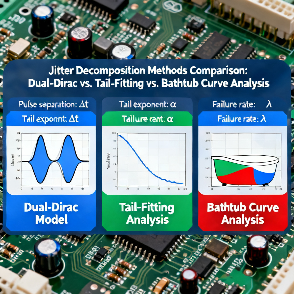
The Dual-Dirac Model (Standard)
- Assumes the jitter histogram has two Gaussian distributions (left and right edges).
- The distance between the means of the two Gaussians = DJ (peak-to-peak).
- The standard deviation of each Gaussian = RJ (rms).
- Limitation: Does not work well for multi-modal jitter (e.g., multiple periodic jitter sources).
Tail-Fitting (Recommended for Accuracy)
- Plot the cumulative distribution function (CDF) of the jitter histogram on a semi-log scale.
- The tails of the CDF will be linear if the jitter is purely Gaussian. Deviation from linearity indicates DJ.
- Fit a straight line to the tails to extract RJ (slope) and DJ (offset).
- Pro Tip from Oscilloscope Manufacturers: Use a BER contour (eye diagram at multiple BER thresholds) to visualize the tail behavior.
Bathtub Curve Analysis
- A bathtub curve plots BER vs. sampling phase (left and right of the eye center).
- The “flat” regions in the middle of the bathtub curve are dominated by DJ. The steep slopes at the edges are dominated by RJ.
- Practical Use: You can read TJ directly from the bathtub curve at BER=10-12. Then, by fitting a model, you extract RJ and DJ.
Frequency-Domain Analysis (Phase Noise)
- Convert jitter to phase noise (dBc/Hz vs. offset frequency).
- RJ appears as a flat noise floor (white phase noise) or a 1/f2 region (random walk).
- PJ appears as discrete spurs.
- Best for: Isolating Periodic Jitter sources (e.g., switching regulator noise at 100 kHz).
Practical PCB Design Guidelines to Minimize Jitter
Based on the decomposition insights, here are actionable steps for your high-speed PCB layout:
- Control Impedance: Use controlled impedance traces (e.g., 50Ω single-ended, 100Ω differential) with a tolerance of ±5%. Impedance mismatches cause reflections → ISI → DDJ.
- Minimize Stubs: Backdrill vias to remove unused stub lengths. Every stub acts as a resonant cavity that adds DDJ.
- Use Low-Loss Dielectrics: For 10+ Gbps, FR-4 is insufficient. Use materials like Rogers 4350B, Isola Tachyon, or Megtron 6 to reduce dielectric absorption (which causes ISI).
- Power Integrity is Signal Integrity: Place decoupling capacitors close to the IC power pins. Use a solid power plane to reduce ripple-induced PJ.
- Differential Pair Skew: Match trace lengths within 5 mils (0.127 mm). Skew causes DCD.
- Crosstalk Management: Keep a 3W spacing (3x trace width) between high-speed traces. Use ground vias as stitching fences between lanes.
- Clock Distribution: Use dedicated clock layers (not shared with data). Terminate clock traces with series resistors to reduce reflections.
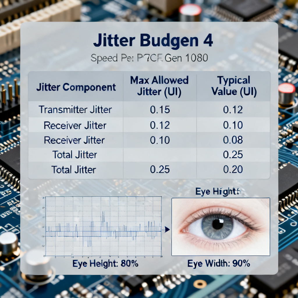
Jitter Budget Example (PCIe Gen 4)
For a 16 GT/s PCIe Gen 4 link (UI = 62.5 ps):
| Component | Budget (ps) | Source |
|---|---|---|
| TJ at BER=10-12 | 31.25 ps (0.5 UI) | Standard |
| DJ (p-p) | 15 ps | TX + Channel |
| RJ (rms) | 1.0 ps | TX + RX PLL |
| RJ (p-p at BER=10-12) | 2 × 7.44 × 1.0 = 14.88 ps | Calculation |
| Total (DJ + RJ) | 29.88 ps | Within budget |
If your measured DJ is 20 ps and RJ is 1.2 ps rms, you exceed the budget (20 + 2×7.44×1.2 = 37.86 ps). Decomposition tells you to fix DJ (e.g., improve channel loss) first.
Conclusion: From Measurement to Design
Jitter decomposition is not an academic exercise—it is the bridge between a failing eye diagram and a successful high-speed PCB. By understanding that Total Jitter = Deterministic (bounded, fixable) + Random (unbounded, manageable), you can prioritize your design efforts.
- If DJ dominates: Fix your channel (impedance, loss, crosstalk).
- If RJ dominates: Improve your power delivery and clock source.
For your next 25 Gbps or 56 Gbps design, invest in a good real-time oscilloscope (e.g., Keysight Infiniium UXR, Tektronix DPO70000SX) with jitter decomposition software. Run bathtub curves, tail-fitting, and phase noise analysis. Then, apply the PCB guidelines above.
Need help designing a low-jitter, high-speed PCB? Contact our engineering team. We specialize in stackup optimization, impedance control, and signal integrity simulation for your custom PCB manufacturing needs.
Frequently Asked Questions (FAQ)
What is jitter decomposition in eye diagram PCB?
Jitter decomposition in eye diagram PCB is the process of separating total jitter into its fundamental components: Random Jitter (RJ), Deterministic Jitter (DJ), and Total Jitter (TJ). This analysis is critical for diagnosing signal integrity issues in high-speed designs.
How does random jitter differ from deterministic jitter?
Random jitter is unbounded and Gaussian, caused by thermal or shot noise, while deterministic jitter is bounded and predictable, arising from sources like ISI, crosstalk, or power supply noise. Jitter decomposition in eye diagram PCB relies on this distinction for accurate modeling.
What tools are used for jitter decomposition?
Engineers use real-time oscilloscopes with jitter analysis software, bathtub curve analysis, tail-fitting algorithms, and phase noise measurements to perform jitter decomposition in eye diagram PCB. These tools help separate RJ, DJ, and TJ for compliance testing.
Why is jitter decomposition important for high-speed PCB design?
Jitter decomposition in eye diagram PCB is essential for meeting standards like PCIe Gen 5 and 100G Ethernet. It allows designers to identify root causes of timing errors, optimize PCB layout, and ensure reliable data transmission at high speeds.