[rank_math_breadcrumb]
Automating jitter in high speed PCB measurements using Python and SCPI commands transforms manual timing analysis into a repeatable, data-driven process. This guide consolidates expert techniques from leading test equipment manufacturers to help you measure, analyze, and reduce jitter in your high-speed designs efficiently.
Jitter Fundamentals for High Speed PCB Measurements
Jitter—the deviation from ideal timing in digital signals—is a critical performance metric in high speed PCB design. As data rates push beyond 10 Gbps, manual jitter measurement becomes impractical, error-prone, and time-consuming. Automating these measurements with Python and Standard Commands for Programmable Instrumentation (SCPI) not only increases accuracy but also accelerates your design iteration cycle.
Types of Jitter in High Speed PCB Measurements
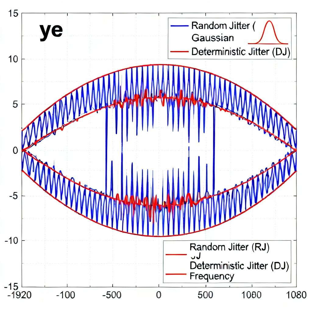
| Jitter Type | Description | Source in High Speed PCB Measurements |
|---|---|---|
| Random Jitter (RJ) | Gaussian, unbounded | Thermal noise, shot noise |
| Deterministic Jitter (DJ) | Bounded, predictable | Crosstalk, duty-cycle distortion, ISI |
| Total Jitter (TJ) | Combination at BER 10^-12 | Extrapolated from RJ and DJ |
Why Automate Jitter in High Speed PCB Measurements?
Manual measurement with an oscilloscope is subjective and slow. Automation allows you to capture thousands of edges, perform statistical analysis, and generate compliance reports (e.g., for PCIe or USB standards) in minutes.
Setting Up Automated Jitter Measurement Environment for High Speed PCB
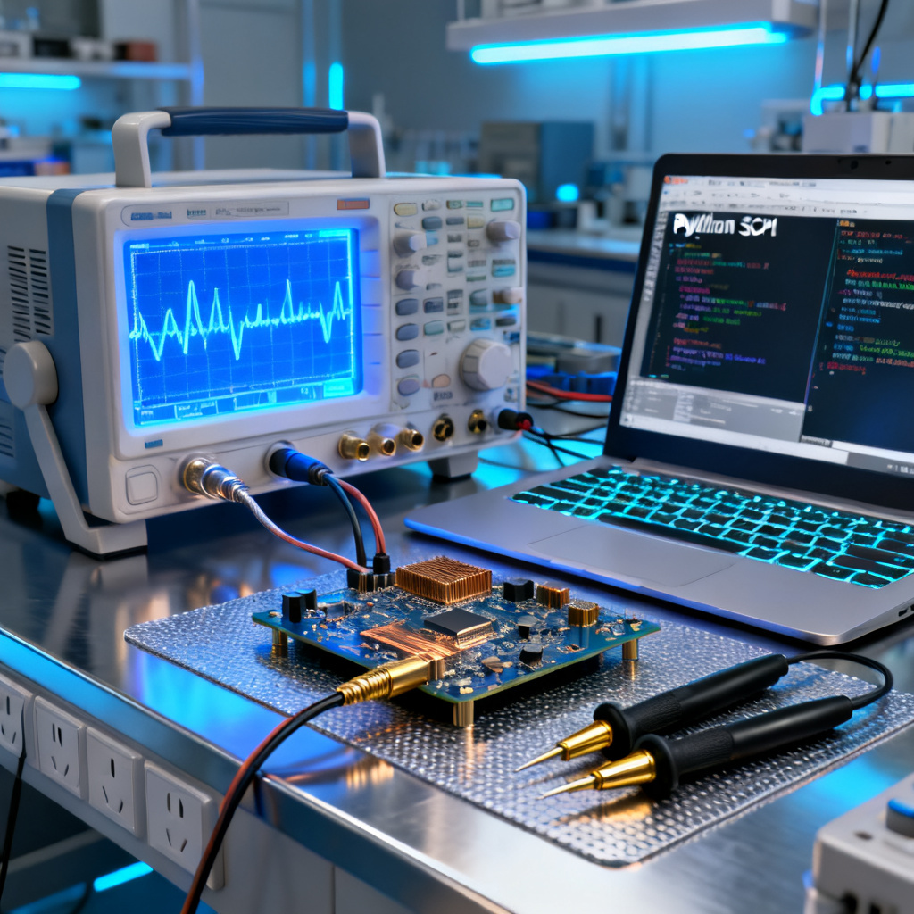
To automate jitter in high speed PCB measurements, you need three components: a high-bandwidth oscilloscope (≥ 4 GHz), a Python environment (3.8+) with pyvisa, numpy, matplotlib, scipy, and SCPI commands for instrument control.
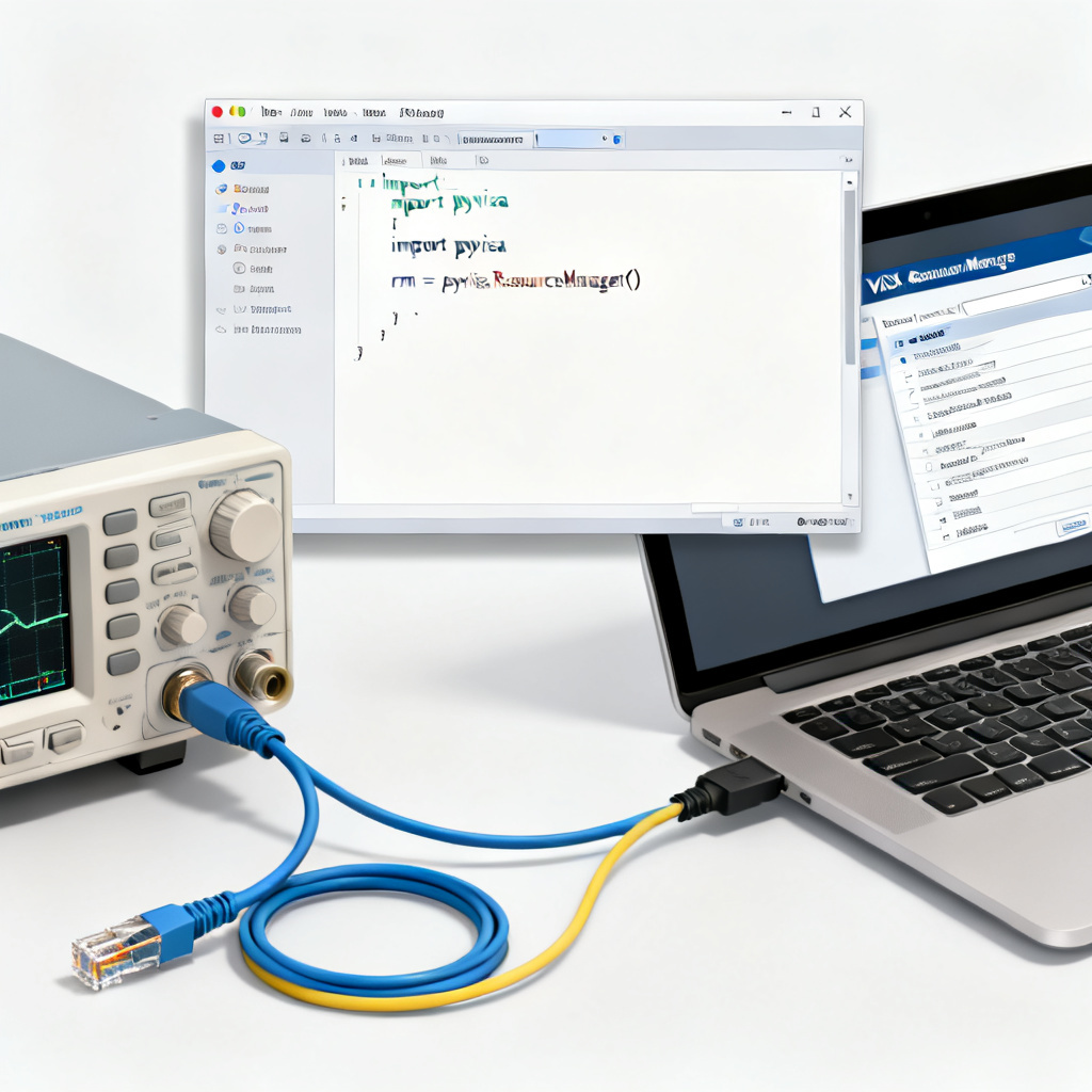
Step 1: Install PyVISA and Connect to Your Scope
import pyvisa
import numpy as np
import matplotlib.pyplot as plt
from scipy import stats

rm = pyvisa.ResourceManager()
scope = rm.open_resource('TCPIP0::192.168.1.100::inst0::INSTR')
scope.timeout = 10000
print(scope.query('*IDN?'))
Step 2: Configure the Oscilloscope for Jitter Measurement
scope.write(':TIMebase:SCALe 100e-12')
scope.write(':TIMebase:POSition 50e-9')
scope.write(':TRIGger:EDGE:SOURce CH1')
scope.write(':TRIGger:EDGE:LEVel 0.5')
scope.write(':TRIGger:EDGE:SLOPe POS')
scope.write(':MEASure:JITTer:ENABle ON')
scope.write(':MEASure:JITTer:TYPE TJ')
Step 3: Capture Waveform Data for Jitter Analysis
scope.write(':ACQuire:STOPAfter RUNSTop')
scope.write(':RUN')
import time
time.sleep(2)
scope.write(':WAVeform:FORMat ASCII')
scope.write(':WAVeform:SOURce CH1')
data = scope.query_ascii_values(':WAVeform:DATA?')
time_axis = np.linspace(0, len(data)*100e-12, len(data))
Step 4: Extract Edge Timings for Jitter Calculation
amplitude = np.max(data) - np.min(data)
threshold = np.min(data) + 0.5 * amplitude
edges = []
for i in range(1, len(data)):
    if data[i-1] < threshold and data[i] >= threshold:
        t_cross = time_axis[i-1] + (threshold - data[i-1]) * (time_axis[i] - time_axis[i-1]) / (data[i] - data[i-1])
        edges.append(t_cross)
ideal_period = 1e-9
tie = [(edges[i] - edges[0] - i * ideal_period) for i in range(len(edges))]
Step 5: Calculate Jitter Parameters
rj = np.std(tie) * 1e12
dj = (np.max(tie) - np.min(tie)) * 1e12 - 2 * rj
q_factor = 7.08
tj = (dj + 2 * q_factor * rj) * 1e12
print(f"RJ (RMS): {rj:.2f} ps")
print(f"DJ (pk-pk): {dj:.2f} ps")
print(f"TJ @ BER 1e-12: {tj:.2f} ps")
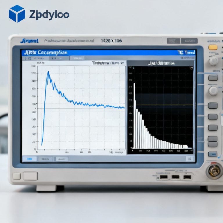
Step 6: Visualize the Jitter Distribution
plt.figure(figsize=(10, 6))
plt.hist(tie, bins=50, density=True, alpha=0.7, label='Measured TIE')
mu, std = stats.norm.fit(tie)
x = np.linspace(min(tie), max(tie), 100)
plt.plot(x, stats.norm.pdf(x, mu, std), 'r--', label=f'Gaussian fit (RJ = {std*1e12:.2f} ps)')
plt.xlabel('Time Interval Error (TIE) [s]')
plt.ylabel('Probability Density')
plt.title('Jitter Distribution for High Speed PCB Measurement')
plt.legend()
plt.grid(True)
plt.savefig('jitter_histogram.png')
plt.show()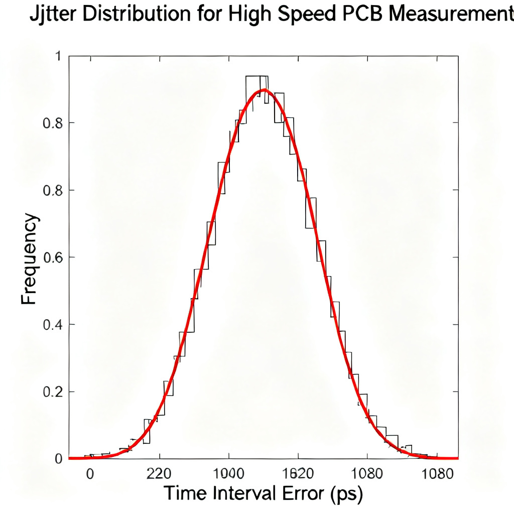
Advanced Techniques for Accurate Jitter Automation in High Speed PCB
Advanced jitter automation in high speed PCB measurements includes de-embedding test fixtures, filtering low-frequency wander, and performing compliance testing against industry standards.
De-Embedding and Filtering
scope.write(':DEEMbed:STATe ON')
scope.write(':DEEMbed:FILE "C:\\fixture_s4p.s4p"')
scope.write(':DEEMbed:APPLy')

from scipy.signal import butter, filtfilt
def highpass_filter(data, cutoff=1e6, fs=1e10):
    nyq = 0.5 * fs
    normal_cutoff = cutoff / nyq
    b, a = butter(1, normal_cutoff, btype='high', analog=False)
    return filtfilt(b, a, data)
tie_filtered = highpass_filter(tie)
Compliance Testing for High Speed PCB Standards
ui = 1e-9
tj_limit = 0.3 * ui * 1e12
dj_limit = 0.15 * ui * 1e12
if tj < tj_limit and dj < dj_limit:
    print("PASS: Jitter within PCIe Gen 5 specifications")
else:
    print("FAIL: Jitter exceeds limits")
Batch Automation for Design Iteration
test_rates = [1e9, 2.5e9, 5e9, 10e9]
results = []
for rate in test_rates:
    scope.write(f':SOURce:DATA:RATE {rate}')
    time.sleep(1)
    # Reuse measurement code
    results.append({'rate': rate, 'TJ': tj, 'RJ': rj, 'DJ': dj})
import csv
with open('jitter_results.csv', 'w', newline='') as f:
    writer = csv.DictWriter(f, fieldnames=['rate', 'TJ', 'RJ', 'DJ'])
    writer.writeheader()
    writer.writerows(results)
Troubleshooting Common Issues in Jitter Automation for High Speed PCB
| Issue | Cause | Solution |
|---|---|---|
| High RJ but clean signal | Noise from scope probe or ground loop | Use active probes, ensure proper grounding, add ferrite beads |
| DJ > 10 ps | Crosstalk from adjacent traces | Increase spacing, add guard traces in PCB layout |
| TIE histogram shows two peaks | Duty-cycle distortion (DCD) | Check clock duty cycle, adjust rise/fall times |
| SCPI connection timeout | Incorrect IP or VISA driver | Verify scope IP, install NI-VISA or pyvisa-py |
| Measurement varies between runs | Insufficient number of edges captured | Increase acquisition points (e.g., 500,000 points) |
Best Practices for High Speed PCB Design to Minimize Jitter
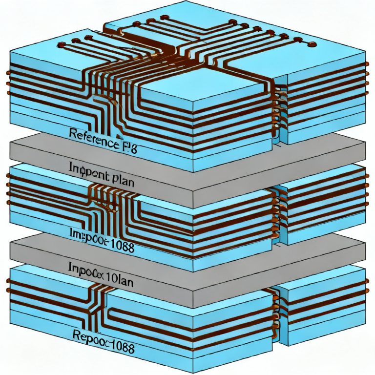
While automation helps measure jitter, the ultimate goal is to design it out. Key high speed PCB design considerations include impedance control within ±10%, minimizing stubs using microvias, ensuring power integrity with decoupling capacitors, using differential clocks with matched trace lengths, and performing SI simulation before fabrication.
Frequently Asked Questions About Jitter Automation in High Speed PCB Measurements
What is jitter automation in high speed PCB measurements?
How does Python SCPI help with jitter analysis for high speed PCBs?
What equipment is needed for automated jitter measurement in high speed PCBs?
Comparison: Manual vs Automated Jitter Measurement for High Speed PCB
| Aspect | Manual Jitter Measurement | Automated Jitter Measurement Using Python SCPI |
|---|---|---|
| Speed | Slow, subjective | Fast, repeatable |
| Accuracy | Limited by human error | High precision, statistical |
| Data Volume | Few edges | Thousands of edges |
| Compliance Reporting | Manual calculation | Automated pass/fail |
| Design Iteration | Time-consuming | Batch processing |
Glossary of Jitter and High Speed PCB Terms
- Jitter: Time-domain uncertainty of digital signal edge transitions.
- Random Jitter (RJ): Gaussian jitter from thermal noise, unbounded.
- Deterministic Jitter (DJ): Bounded jitter from crosstalk, ISI, DCD.
- Total Jitter (TJ): Combined RJ and DJ at a given BER.
- SCPI: Standard Commands for Programmable Instrumentation.
- TIE: Time Interval Error, the deviation from ideal edge timing.
- De-embedding: Removing test fixture effects from measurements.