In High Speed PCB design, jitter in eye diagram analysis reveals critical signal integrity insights. The open and close of the eye directly indicate timing margin, noise levels, and data reliability. This guide explains how to interpret these visual cues for robust high-speed performance.
Master High-Speed PCB design with our in-depth guide to jitter analysis using eye diagrams. Learn what the open and close of the eye reveal about signal integrity, timing margin, and PCB performance. Expert insights for B2B engineers.
Fundamentals of Jitter and Eye Diagrams in High Speed PCB
What Is an Eye Diagram in High Speed PCB?
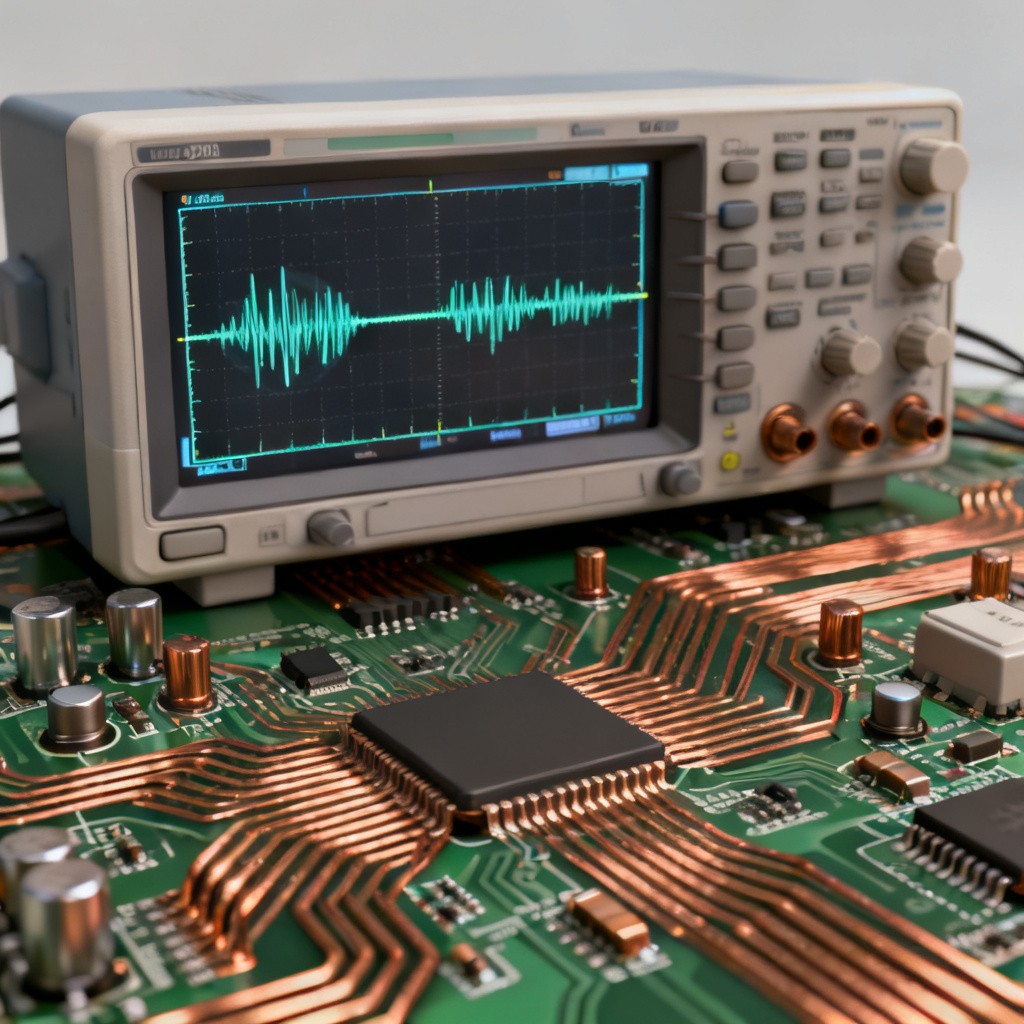
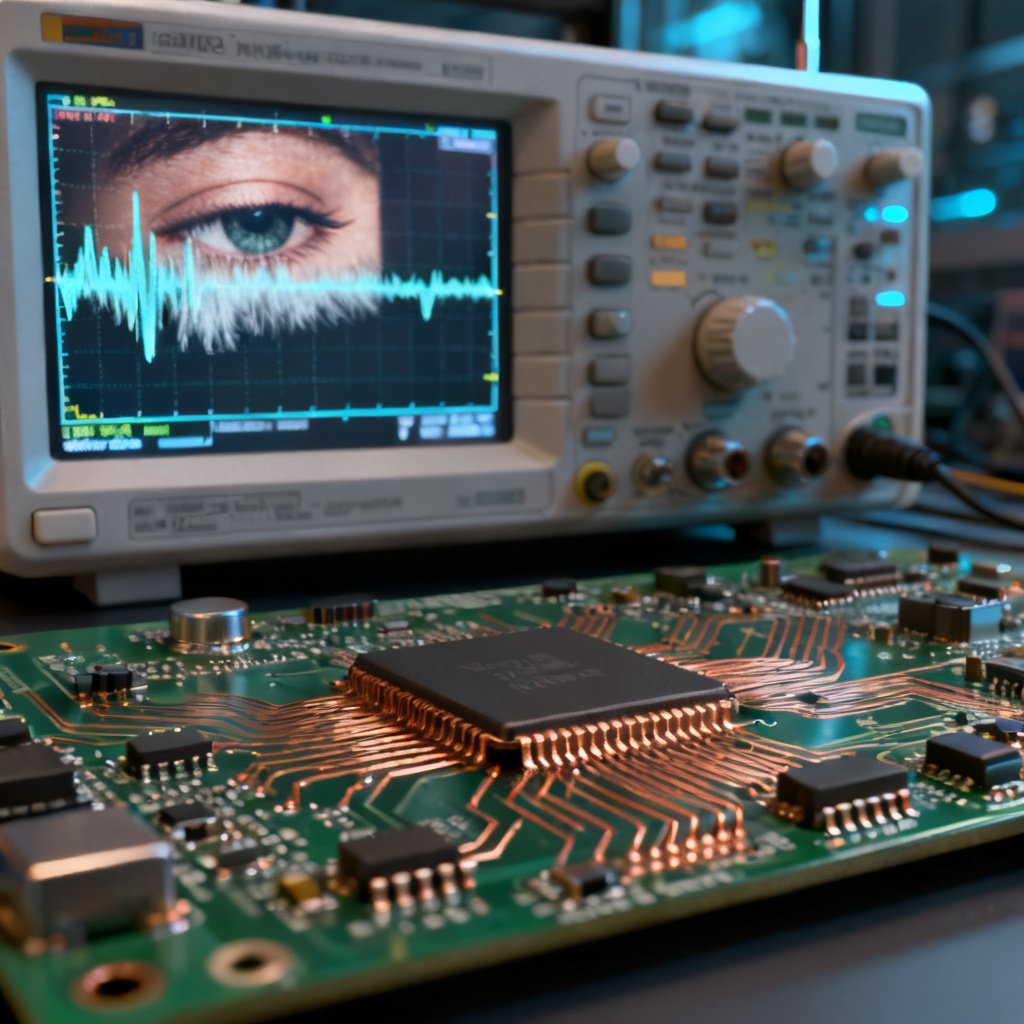
An eye diagram in High Speed PCB is created by overlaying many short segments of a digital signal onto a single oscilloscope display. The resulting pattern looks like a human eye. It provides a statistical view of signal transitions, showing how voltage levels and timing vary over many bits.
Key components of an eye diagram include:
- Eye Opening (Vertical): Represents the voltage margin between logic ‘1’ and ‘0’.
- Eye Opening (Horizontal): Represents the time margin or timing window during which the signal is stable.
- Eye Height: The difference between the mean ‘1’ level and the mean ‘0’ level, minus noise.
- Eye Width: The time interval during which the signal is valid, free from transition edges.
- Crossing Point (or Zero Crossing): The point where rising and falling edges intersect; its position indicates duty cycle distortion.
What Is Jitter in High Speed PCB?
Jitter in High Speed PCB is defined as the deviation of a signal’s significant instants (e.g., rising/falling edges) from their ideal positions in time. It is the primary cause of horizontal eye closure. Jitter is typically measured in picoseconds (ps) or Unit Intervals (UI).
There are two fundamental categories of jitter:
- Random Jitter (RJ): Unbounded, Gaussian-distributed jitter caused by thermal noise, shot noise, and other stochastic processes. It cannot be eliminated, only minimized.
- Deterministic Jitter (DJ): Bounded and predictable jitter caused by specific, identifiable sources. It is further divided into:
- Data-Dependent Jitter (DDJ): Includes Inter-Symbol Interference (ISI) and Duty Cycle Distortion (DCD).
- Periodic Jitter (PJ): Caused by external noise sources like power supply ripple or crosstalk.
- Bounded Uncorrelated Jitter (BUJ): Caused by random but bounded events like switching noise.
Why jitter matters in High Speed PCB: At high data rates, the timing budget (the available time to sample a bit) shrinks. If jitter consumes too much of this budget, the receiver cannot reliably distinguish a ‘1’ from a ‘0’. This leads to bit errors, data corruption, and system failure.
What the Open and Close of the Eye Tell You in High Speed PCB
The Open Eye: The Goal of High Speed PCB Design
A healthy, open eye diagram indicates excellent signal integrity. It tells you:
- Sufficient Voltage Margin: The eye is tall, meaning the signal has enough amplitude to be reliably detected despite noise.
- Sufficient Timing Margin: The eye is wide horizontally, meaning there is a large window of stability where the receiver can sample the data without errors.
- Low jitter: The transition edges are sharp and consistent. The overlapping traces are thin and tightly clustered at the crossing points. This indicates minimal timing uncertainty.
- Minimal ISI: The eye is “clean” with no significant “ghost” traces or multiple levels inside the eye opening. Previous bits do not significantly distort the current bit.
- Symmetry: The crossing point is at 50% of the signal amplitude, indicating a balanced duty cycle (no DCD).
The Closing Eye: Diagnosing Problems in High Speed PCB
A closed or partially closed eye is a red flag. The specific characteristics of the closure point to root causes.
- Horizontal Eye Closure (Narrow Eye Width):
- Primary Cause: High jitter.
- Interpretation: The timing window for sampling is shrinking. This is the most common failure mode in high-speed links.
- Specific Clues:
- Thick, fuzzy transition edges: Indicates significant RJ and/or PJ.
- Multiple distinct traces at the crossing point: Indicates DDJ, especially ISI. You may see two or more distinct “bathtub” curves at the crossing.
- Widely spread crossing point: Indicates high total jitter (TJ).
- Vertical Eye Closure (Short Eye Height):
- Primary Cause: Noise, attenuation, or impedance mismatch.
- Interpretation: The voltage difference between ‘1’ and ‘0’ is too small. This can be caused by:
- Signal Attenuation: High-frequency losses in the PCB trace (skin effect, dielectric loss).
- Crosstalk: Noise coupled from adjacent traces.
- Power Supply Noise (PSRR): Noise on the power rail modulates the signal amplitude.
- Reflections: Impedance discontinuities cause voltage levels to bounce.
- Asymmetric Eye (Tilted or Slanted):
- Primary Cause: Duty Cycle Distortion (DCD).
- Interpretation: The crossing point is not at 50% (e.g., it is at 40% or 60%). This indicates that the ‘1’ and ‘0’ pulses have different widths.
- Root Causes:
- Driver Asymmetry: The rise time and fall time of the transmitter are different.
- Threshold Offset: The receiver’s threshold voltage is not at the midpoint of the signal swing.
- Double or Multiple Eyes (Ghost Traces):
- Primary Cause: Inter-Symbol Interference (ISI).
- Interpretation: The eye diagram shows multiple distinct levels or “eyes” stacked on top of each other. This is a classic sign of ISI, where the signal’s history (previous bits) affects the current bit’s voltage.
- Root Causes:
- Bandwidth Limitation: The PCB trace or connector acts as a low-pass filter, slowing down transitions.
- Impedance Mismatch: Reflections cause the signal to “ring” and not settle in time.
- Long Stubs: Unterminated branches on the trace create reflections that interfere with the main signal.
Root Causes of Jitter in High Speed PCB Designs
To fix jitter in High Speed PCB, you must understand its origins. Here are the most common sources in a PCB environment.
Impedance Discontinuities and Reflections in High Speed PCB
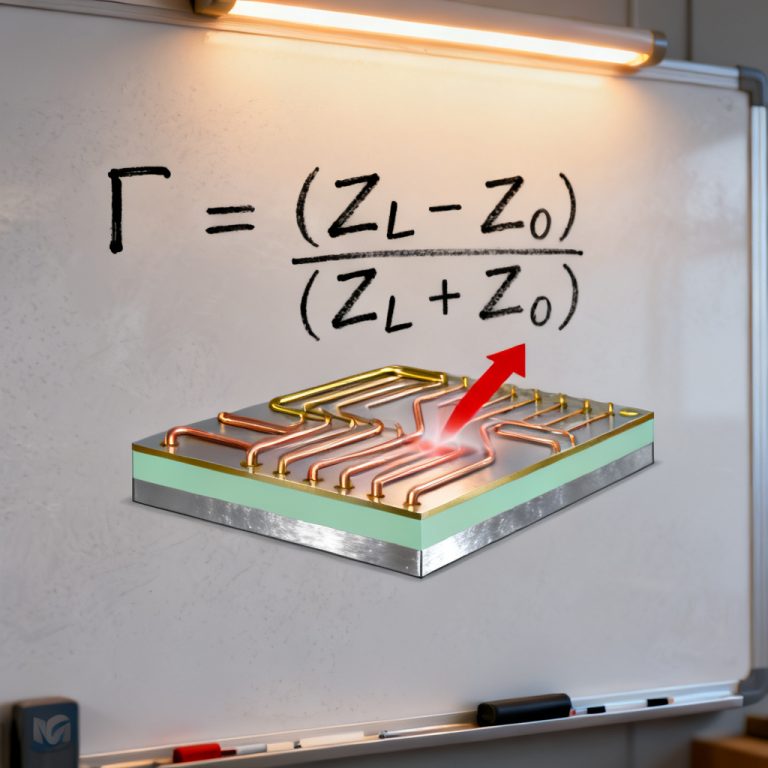
Any change in the characteristic impedance of the transmission line (e.g., at vias, connectors, BGA breakout regions, or changes in trace width) will cause a reflection. This reflection travels back to the source and then back to the receiver, arriving after the main signal. This delayed energy creates ISI, increasing jitter.
- How to Mitigate: Use controlled impedance traces. Minimize the number of vias. Use proper via stitching and back-drilling to reduce stub length. Match the impedance of the driver, trace, and receiver.
Crosstalk in High Speed PCB
Crosstalk is the unwanted coupling of energy from one signal line (the aggressor) to an adjacent line (the victim). It can be capacitive (edge-to-edge) or inductive (loop-to-loop). Crosstalk noise adds to the victim signal’s voltage, causing vertical eye closure, and also modulates its timing, causing jitter.
- How to Mitigate: Increase spacing between traces (the 3W rule is a good start). Use differential signaling (which inherently rejects common-mode noise). Route critical high-speed signals on inner layers between ground planes. Use guard traces.
Power Supply Noise (PSRR) in High Speed PCB
Noise on the power supply rails (e.g., from switching regulators or other digital activity) couples directly into the signal output of the driver. This modulates the driver’s switching speed, causing Periodic Jitter (PJ) and Random Jitter (RJ).
- How to Mitigate: Use dedicated, low-noise power planes. Place decoupling capacitors (bulk and high-frequency) close to the power pins of active devices. Use ferrite beads to isolate noisy power domains. Ensure proper PDN (Power Distribution Network) design.
Skin Effect and Dielectric Loss in High Speed PCB
At high frequencies, the current in a trace flows only on its surface (skin effect), increasing resistance. The PCB substrate material also absorbs some of the signal energy (dielectric loss). These losses attenuate the signal amplitude and slow down the rise/fall times, leading to ISI and vertical eye closure.
- How to Mitigate: Use low-loss PCB materials (e.g., Rogers, Megtron, Isola). Use wider traces to reduce resistance (if impedance allows). Use pre-emphasis or de-emphasis at the transmitter to boost high-frequency content.
Clock Jitter and Phase Noise in High Speed PCB
Jitter in the reference clock (from the oscillator or PLL) is directly transferred to the data signal. This is a primary source of PJ and RJ.
- How to Mitigate: Use low-jitter crystal oscillators. Use clean, dedicated power for clock generation circuits. Keep clock traces short and shielded from other signals.
Advanced Analysis: Jitter Decomposition and Bathtub Curves for High Speed PCB
Jitter Decomposition in High Speed PCB
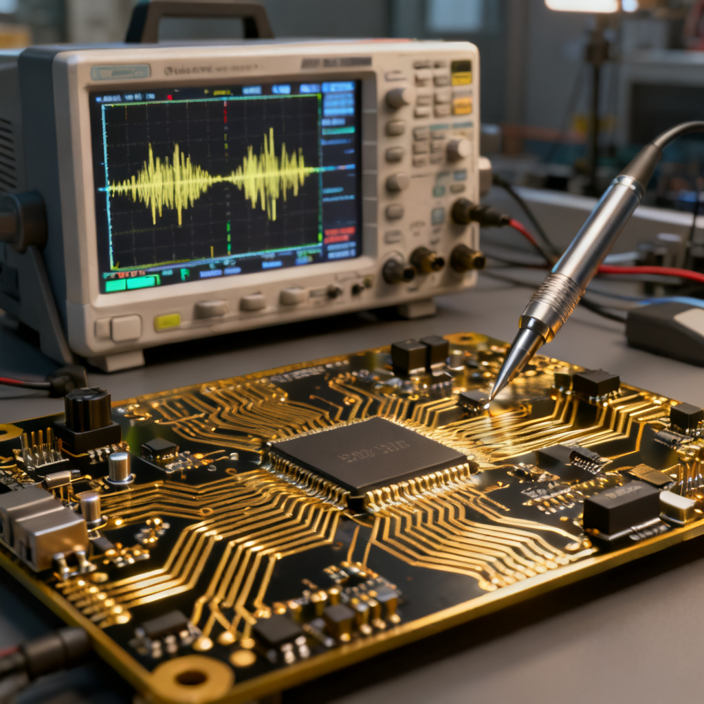
To effectively troubleshoot jitter in High Speed PCB, you must separate total jitter (TJ) into its components. Modern oscilloscopes with dedicated jitter analysis software can perform this decomposition.
- TIE (Time Interval Error): The fundamental measurement. It measures the difference between the actual edge position and the ideal edge position.
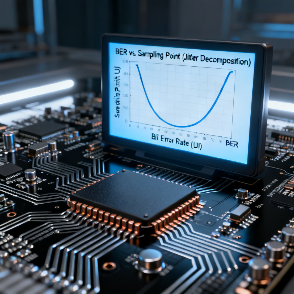
- Bathtub Curve: A plot of bit error rate (BER) versus sampling point. The left and right sides of the “bathtub” represent the probability of a bit error due to jitter on the left and right edges of the eye. The flat bottom of the curve is the eye opening at a given BER.
- The Dual-Dirac Model: A common method to estimate TJ. It models RJ as a Gaussian distribution and DJ as two delta functions. The formula is: TJ = DJ + 2α × RJ, where α is a factor based on the target BER (e.g., α = 14.069 for BER = 1e-12).
What Bathtub Curves Tell You in High Speed PCB
- Steep Slopes: Indicates that DJ is the dominant component. The eye closure is primarily due to bounded, predictable jitter (e.g., from crosstalk or ISI).
- Gradual Slopes: Indicates that RJ is the dominant component. The jitter is predominantly random (e.g., from thermal noise or a noisy PLL).
- Narrow Bottom: The eye is closing quickly as the BER requirement tightens. This means the deterministic jitter is large.
- Wide Bottom: The eye remains open even at very low BER, indicating that the jitter is mostly random and the deterministic component is small.
The Importance of BER in High Speed PCB
An eye diagram is a visual tool, but a Bathtub curve is a quantitative one. For a high-speed link, you typically need a BER of 1e-12 or better. The eye diagram you see on the screen may look open, but the bathtub curve will tell you if it is truly open at the required BER.
Practical Troubleshooting: From Eye Diagram to Root Cause in High Speed PCB
Here is a step-by-step guide to using the eye diagram for troubleshooting jitter in High Speed PCB.
Step 1: Visual Inspection
- Is the eye open? Yes? Good. No? Proceed.
- Is the closure vertical or horizontal? This is your first clue.
Step 2: Horizontal Closure Analysis
- Measure TIE Jitter: Get the TIE histogram. Is it Gaussian (RJ) or bimodal (DJ)?
- Look at the Bathtub Curve: Are the slopes steep (DJ) or gradual (RJ)?
- If DJ is dominant:
- Check for ISI: Look for ghost traces in the eye. Check the trace length and impedance. Look for long stubs.
- Check for PJ: Look for a sinusoidal pattern in the TIE trend. Check your power supply for ripple at a specific frequency.
- Check for DCD: Measure the duty cycle. Is it 50%? Check the driver’s rise/fall time symmetry.
Step 3: Vertical Closure Analysis
- Measure Eye Height: Is it above the receiver’s input threshold?
- Check for Noise: Look for noise on the top and bottom of the eye. Is it bounded (crosstalk) or random (thermal)?
- Check for Attenuation: Measure the signal amplitude at the transmitter and receiver. Is it significantly lower at the receiver? This indicates loss.
Step 4: Mitigation Actions
- For ISI: Shorten trace length. Remove stubs. Use better PCB materials. Apply pre-emphasis/de-emphasis.
- For Crosstalk: Increase trace spacing. Use differential signaling. Add guard traces.
- For Power Supply Noise: Improve decoupling. Use a low-noise LDO for sensitive circuits. Add a ferrite bead.
- For Reflections: Fix impedance mismatches. Use series termination at the source or parallel termination at the load.
Jitter Mitigation Techniques in High Speed PCB: Structured Table
| Jitter Source in High Speed PCB | Root Cause | Mitigation Technique |
|---|---|---|
| Inter-Symbol Interference (ISI) | Bandwidth limitation, impedance mismatch, long stubs | Shorten trace length, remove stubs, use low-loss materials, apply pre-emphasis |
| Crosstalk | Capacitive/inductive coupling between traces | Increase trace spacing (3W rule), use differential signaling, guard traces |
| Power Supply Noise | Switching regulator ripple, digital noise | Decoupling capacitors, low-noise LDO, ferrite beads, proper PDN design |
| Impedance Discontinuity | Vias, connectors, BGA breakout, trace width change | Controlled impedance, minimize vias, back-drilling, series/parallel termination |
| Clock Jitter | Noisy oscillator or PLL | Low-jitter crystal oscillator, clean power for clock, short shielded traces |
High Speed PCB Jitter Analysis: Open vs Closed Eye Comparison
Understanding the difference between an open and closed eye in High Speed PCB jitter analysis is critical for design validation. An open eye indicates robust signal integrity with sufficient timing and voltage margin, while a closed eye signals degradation requiring immediate attention. Our advanced manufacturing processes, controlled impedance capabilities, and strict quality control ensure that your designs achieve the open, clean eye diagrams they require. Partner with us for your next High Speed PCB project to minimize jitter and maximize performance.
FAQ: Jitter in High Speed PCB Eye Diagram Analysis
What does jitter in High Speed PCB eye diagram analysis indicate?
Jitter in High Speed PCB eye diagram analysis indicates timing uncertainty in signal transitions, which directly causes horizontal eye closure and reduces the timing margin available for reliable data sampling.
How can I reduce jitter in High Speed PCB designs?
To reduce jitter in High Speed PCB designs, focus on controlled impedance routing, minimize crosstalk through proper spacing and shielding, use low-noise power supplies, and select low-loss PCB materials to mitigate ISI and attenuation.
Why is the eye diagram important for High Speed PCB signal integrity?
The eye diagram is important for High Speed PCB signal integrity because it provides a visual representation of voltage and timing margins, allowing engineers to quickly diagnose issues like jitter, noise, and impedance mismatches that can lead to bit errors.
What is the difference between random and deterministic jitter in High Speed PCB?
In High Speed PCB, random jitter (RJ) is unbounded and Gaussian, caused by thermal noise, while deterministic jitter (DJ) is bounded and predictable, caused by specific sources like crosstalk, ISI, or power supply noise. DJ is often easier to mitigate through design improvements.
How does crosstalk affect the eye diagram in High Speed PCB?
Crosstalk in High Speed PCB adds noise to the victim signal, causing vertical eye closure and modulating timing, which increases jitter. This results in a narrower, shorter eye with potential ghost traces, degrading signal integrity.