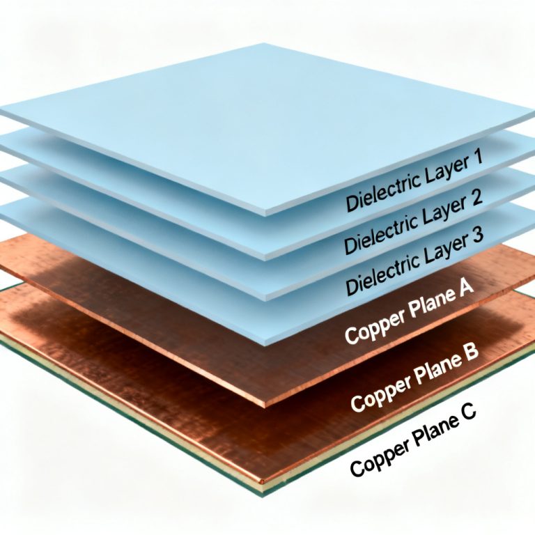
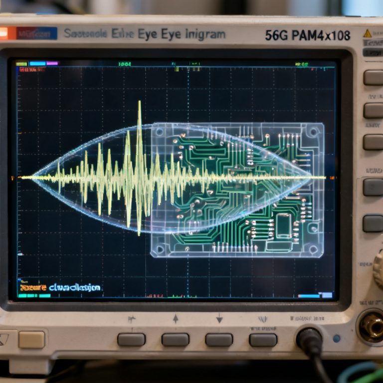
In the world of high-speed digital design—especially for advanced PCBs used in 5G, data centers, and automotive electronics—signal integrity (SI) is non-negotiable. When a high-speed link fails, the eye diagram is your first and most powerful diagnostic tool. This pillar page will teach you exactly how to read, measure, and act on eye diagram results to identify root causes of link failures, optimize your PCB layout, and ensure reliable production.
What Is an Eye Diagram and Why It Matters for PCB Debugging
1.1 The Fundamental Concept
An eye diagram PCB is a synchronized, overlapped display of a digital signal’s transitions over a unit interval. It is created by sampling the signal at the symbol rate and overlaying thousands of bits on an oscilloscope. The resulting pattern looks like an open “eye.”
Why it matters for PCB debug:
- Instant visual health check: A wide-open, clean eye means the link is robust. A closed, noisy, or jittery eye indicates a problem.
- Quantifies margin: The eye opening (both vertical and horizontal) directly tells you how much noise and timing margin your link has before bit errors occur.
- Reveals failure mechanisms: Different types of eye degradation point to specific PCB issues (e.g., impedance mismatch, crosstalk, power supply noise).
1.2 Key Measurements from the Eye Diagram
When debugging a link failure, focus on these four critical parameters:
| Parameter | What It Measures | Typical Root Cause in PCB |
|---|---|---|
| Eye Height (V_eye) | Voltage margin between logic 1 and 0 at the sampling point. | Attenuation, ISI, crosstalk, insufficient drive strength. |
| Eye Width (T_eye) | Timing margin inside the eye opening. | Jitter (random or deterministic), duty cycle distortion, clock recovery issues. |
| Jitter (RJ/DJ) | Total timing uncertainty. | Power supply noise (PJ), crosstalk (DDJ), EMI, poor termination. |
| Rise/Fall Time | Edge speed. | Overly long stubs, excessive capacitance, incorrect driver impedance. |
How to Set Up an Eye Diagram Measurement on Your PCB
2.1 Equipment You Need
You need a real-time oscilloscope with bandwidth ≥ your signal’s 3rd harmonic, or a sampling oscilloscope for data rates ≥ 10 Gbps. Use an active differential probe with low loading capacitance (< 0.5 pF). For probing, use SMA/coaxial breakouts or direct probing on test points designed into the PCB.
2.2 Best Practices for Probing
Probe at the receiver input because the eye diagram at the transmitter may look perfect, but the receiver sees a degraded version after traveling through the PCB trace. Always use differential probing for differential signals; single-ended probing destroys common-mode rejection and introduces noise. Minimize probe ground lead length to avoid inductive loops that add noise and jitter. Ensure proper termination (e.g., 50Ω single-ended, 100Ω differential) to prevent reflections.
2.3 Oscilloscope Setup Steps
- Connect the probe to the receiver test point.
- Set the time base to 1–2 UI per division (e.g., 100 ps/div for 10 Gbps).
- Set the vertical scale so the signal amplitude fills 60–80% of the screen.
- Trigger on the data clock or use a clock recovery trigger for pattern-dependent jitter analysis.
- Acquire > 10,000 waveforms to build a statistically significant eye.
- Enable persistence to see the full distribution of jitter and noise.
Reading the Eye Diagram: What Each Degradation Tells You
3.1 The “Perfect” Eye
Wide horizontal and vertical opening, sharp transitions, minimal noise on the rails. The link has ample margin. No debug needed.
3.2 Closed Eye (Low Eye Height)
The eye opening is narrow vertically; the 1 and 0 levels almost touch. Possible PCB causes: excessive loss (long traces, high-loss substrate, too many vias), crosstalk (aggressive trace spacing, poor stackup isolation), impedance mismatch (reflections cause voltage ringing). Debug action: perform TDR to find impedance discontinuities, check stackup and trace width for correct Z0, add equalization.
3.3 Narrow Eye (Low Eye Width)
The eye is pinched horizontally; crossing points are noisy. Possible causes: deterministic jitter from asymmetric rise/fall times, periodic jitter from power supply ripple, data-dependent jitter from baseline wander. Debug action: use jitter decomposition to separate RJ and DJ, check PCB power supply decoupling, verify AC coupling capacitor values.
3.4 Double or “Ghost” Eye
Two distinct eyes overlapping, or a secondary opening. Possible causes: reflections from a stub (e.g., via without backdrilling) or incorrect termination. Debug action: remove stubs (backdrill vias), add or adjust series termination resistors, simulate the channel with S-parameters.
3.5 Noisy Rails (Fuzzy Top and Bottom)
The 1 and 0 levels are thick with noise, but transitions are clean. Possible causes: power supply noise (inadequate decoupling) or ground bounce (poor return path design). Debug action: probe the power supply at the IC pin, improve local decoupling, add ground stitching vias.
Step-by-Step Debug Process Using the Eye Diagram
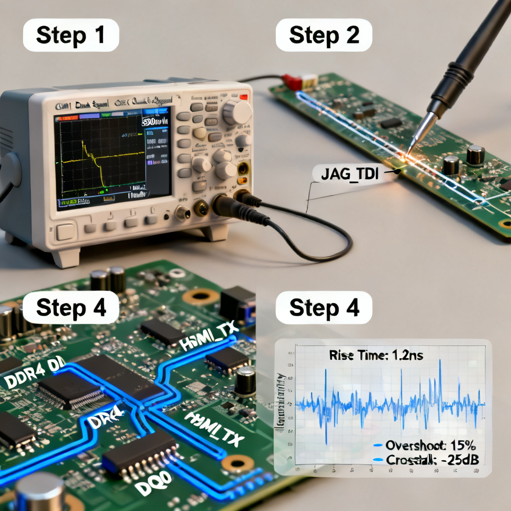
Step 1: Baseline Measurement
Measure the eye at the transmitter output (after the driver but before the PCB trace). This gives you the “best possible” eye and serves as a reference. Record eye height, eye width, and total jitter.
Step 2: Measure at the Receiver Input
Move the probe to the receiver pin on the PCB (after the trace, vias, and connectors). Compare the receiver eye to the transmitter eye. The difference is the channel penalty.
Step 3: Identify the Dominant Degradation
If eye height is the main issue, focus on loss and crosstalk. If eye width is the main issue, focus on jitter and reflections. If both are degraded, it is likely a combination of impedance mismatch and power supply noise.
Step 4: Perform Targeted Debug Actions
For loss: change PCB material (e.g., from FR4 to Megtron 6 or Rogers 4350B), shorten trace length, increase trace width, add pre-emphasis. For crosstalk: increase spacing between aggressor and victim traces, add ground traces, use stripline instead of microstrip. For reflections: backdrill unused via stubs, match termination resistors to trace impedance, use series termination close to the driver. For jitter: add a dedicated power plane for the high-speed IC, use ferrite beads, reduce switching noise from adjacent digital ICs.
Step 5: Re-measure and Iterate
After making a change, re-measure the eye diagram at the receiver. Look for improvement in the specific parameter. If the eye is still closed, go back to Step 3 and try another hypothesis.
Advanced Debugging: Beyond the Basic Eye
5.1 Using Eye Contour Plots
Modern oscilloscopes generate eye contour plots (bathtub curves) that show the probability of error at any timing offset. A steep curve means low jitter; a shallow curve means high jitter. Use this to predict BER without running a full BER test.
5.2 Correlating with S-Parameters
If you have S-parameter measurements of the PCB channel, you can simulate the eye diagram in software (e.g., Keysight ADS, Ansys HFSS). Compare the simulated eye to the measured eye. If they match, your simulation model is accurate. If not, you have a modeling error or an unaccounted-for real-world effect.
5.3 Debugging with Mask Testing
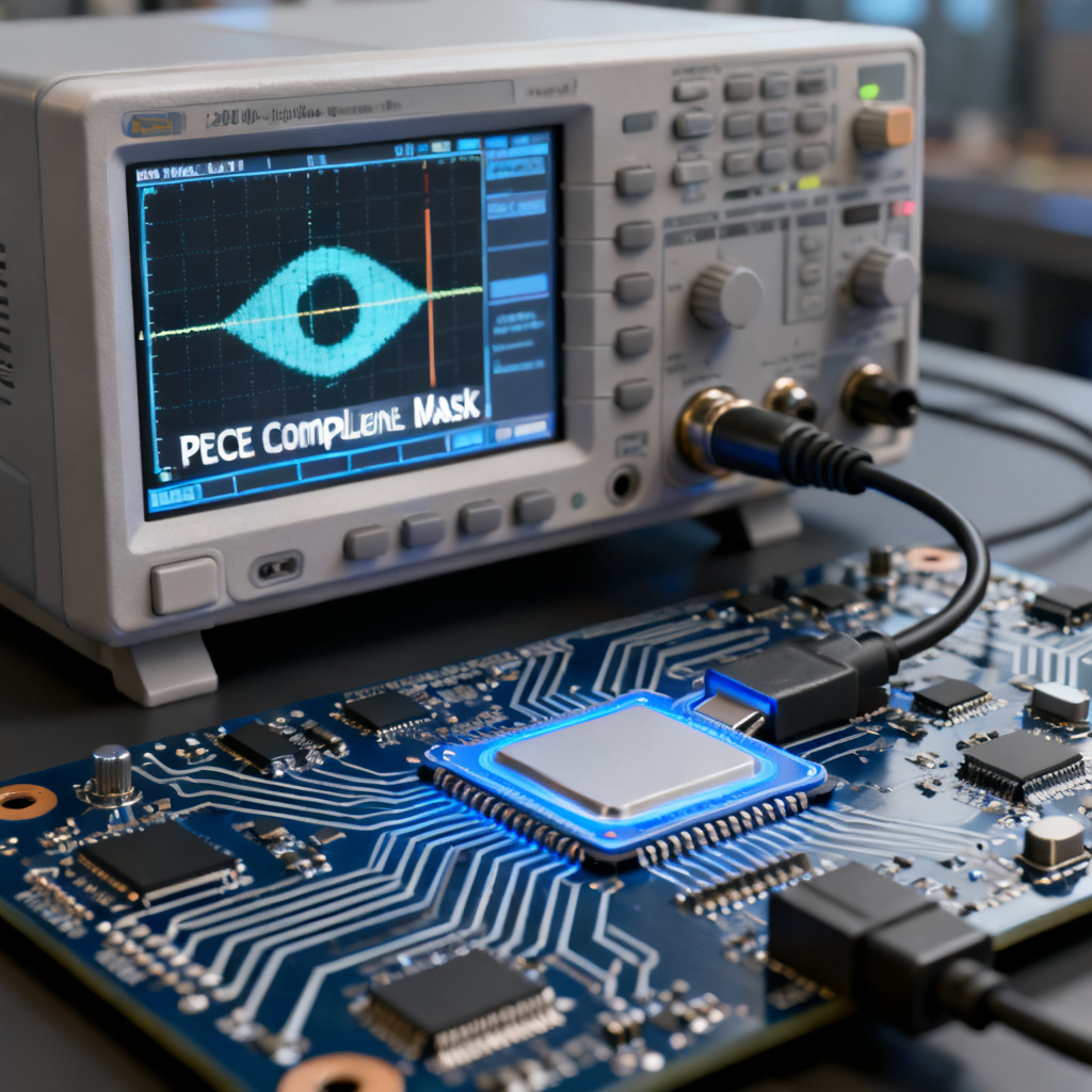
Many standards (e.g., PCIe, USB, Ethernet) define an eye mask – a polygon that the eye must not touch. Use the oscilloscope’s mask test feature to automatically detect failures. If the eye violates the mask, the scope will flag the exact bit pattern and time location of the violation, allowing correlation with a specific PCB layout feature.
Common PCB Design Mistakes That Cause Eye Diagram Failures
| Mistake | Eye Diagram Signature | Fix |
|---|---|---|
| Excessive via stub | Double eye or ghost eye | Backdrill vias or use microvias |
| Poor return path | Noisy rails, increased jitter | Add ground vias next to signal vias |
| AC coupling cap too small | Baseline wander, narrow eye | Increase cap to 100 nF or 1 µF |
| Incorrect trace impedance | Reflections, reduced eye height | Adjust trace width and stackup |
| Crosstalk from adjacent traces | Reduced eye height, increased jitter | Increase spacing or add interleaved ground traces |
| Power supply ripple | Periodic jitter, noisy rails | Improve decoupling, add ferrite bead |
How to Present Eye Diagram Results to Stakeholders
When you find and fix a link failure, document the debug process professionally. Include a summary table with parameters like Eye Height, Eye Width, and Total Jitter before and after the fix. Add three side-by-side eye diagram images: transmitter, receiver before fix, receiver after fix. Write a root cause statement (e.g., “The link failure was caused by a 0.5-inch via stub on the top-layer trace, creating a reflection that reduced the eye width by 40%”). Recommend specific PCB changes (e.g., “Backdrill all vias on Layer 1 to Layer 3 for differential pair DP1-DP2”).
FAQ: Eye Diagram PCB Debug
What is an eye diagram in PCB testing?
An eye diagram PCB is a measurement tool that overlays many digital signal transitions to create an “eye” pattern. It is used to evaluate signal integrity and debug link failures in high-speed PCB designs.
How do I use an eye diagram to debug link failures?
To debug link failures using an eye diagram PCB, measure the eye at the receiver, check for closure (low height/width), identify jitter or noise, and correlate with PCB issues like crosstalk, impedance mismatch, or power supply noise.
What causes a closed eye diagram in high-speed PCBs?
A closed eye diagram PCB is typically caused by excessive loss, crosstalk, impedance mismatch, jitter from power supply noise, or reflections from via stubs. These degrade signal integrity and lead to link failures.