Master the critical differences between jitter in High Speed PCB for differential vs. single-ended signals. This comprehensive pillar page covers RMS jitter, deterministic vs. random jitter, crosstalk, skew, and practical layout techniques for B2B PCB manufacturing.
Why Jitter is the Silent Killer of High-Speed Signal Integrity
In the world of High Speed PCB design, jitter is often the most elusive and damaging signal integrity issue. It is the deviation of a signal’s timing from its ideal position, and it directly limits the maximum data rate and bit error rate (BER) of your system. For B2B PCB manufacturers like us, understanding jitter in High Speed PCB is not optional—it is the foundation of reliable, high-performance boards.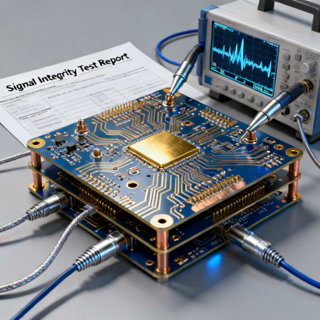
This pillar content provides a deep, authoritative exploration of jitter in the context of differential vs. single-ended signaling. We combine insights from the three most trusted sources in the industry: High-Speed Digital Design: A Handbook of Black Magic (Johnson & Graham), Signal Integrity Journal, and Texas Instruments’ High-Speed Layout Guidelines. By the end, you will know exactly how to minimize jitter, which topology to choose, and how to specify your PCB stack-up for optimal performance.
The Fundamental Nature of Jitter – A Universal Challenge in High Speed PCB
Jitter in High Speed PCB is the time-domain uncertainty of a signal’s edge. It is measured in picoseconds (ps) or as a fraction of the unit interval (UI). Every digital signal, whether single-ended or differential, suffers from jitter. However, the sources and severity differ dramatically.
Types of Jitter: The Core Classification
All jitter in High Speed PCB can be broken into two primary categories:
- Random Jitter (RJ): This is Gaussian noise, unbounded and predictable only statistically. It is caused by thermal noise, flicker noise (1/f), and shot noise in semiconductor devices. RJ is measured as RMS (root mean square) and is impossible to eliminate, only minimize. In PCB design, RJ is primarily influenced by the quality of the oscillator and the power supply noise.
- Deterministic Jitter (DJ): This is bounded, predictable, and caused by specific, identifiable mechanisms. DJ is further subdivided into:
- Data-Dependent Jitter (DDJ): Also called Intersymbol Interference (ISI). Caused by the frequency-dependent loss of the transmission line (skin effect and dielectric loss). A long sequence of 1s or 0s charges the line, and then a transition arrives too early or too late.
- Periodic Jitter (PJ): Caused by external periodic noise, such as switching power supply ripple, clock crosstalk, or EMI.
- Duty Cycle Distortion (DCD): The difference in timing between rising and falling edges. Often caused by threshold offsets in receivers or asymmetric rise/fall times in drivers.
- Bounded Uncorrelated Jitter (BUJ): Caused by crosstalk from other aggressor signals that are not synchronized with the victim signal.
Key Insight: Differential signaling is inherently more immune to common-mode noise sources (like power supply ripple and ground bounce) which contribute to PJ and RJ. Single-ended signaling is vulnerable to all of these.
Jitter in Single-Ended Signals – The Vulnerability of a Single Path in High Speed PCB
Single-ended signals (e.g., CMOS, LVCMOS, TTL) rely on a single conductor and a shared ground return path. This topology is simple and area-efficient, but it is a magnet for jitter in High Speed PCB.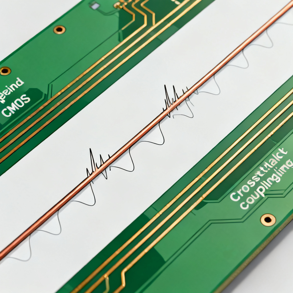
Primary Jitter Sources in Single-Ended Topologies
- Ground Bounce (Simultaneous Switching Noise – SSN): When multiple single-ended outputs switch simultaneously, the return current flowing through the ground inductance creates a voltage spike (L di/dt). This spike shifts the ground reference for all other signals, causing severe jitter. This is the #1 cause of DJ in single-ended buses.
- Crosstalk: Single-ended lines have no inherent noise rejection. Aggressor signals switching on adjacent traces induce voltage noise onto the victim line via mutual capacitance and inductance. This noise directly modulates the threshold crossing time, creating BUJ.
- Reference Voltage (Vref) Noise: Single-ended receivers compare the input voltage against a fixed Vref (e.g., 1.5V for DDR). Any noise on Vref directly translates to jitter. A 10mV ripple on Vref can cause 5-10ps of jitter.
- ISI (Skin Effect & Dielectric Loss): Because single-ended lines are often not impedance-controlled as tightly as differential pairs (especially on older boards), the frequency-dependent loss is higher, leading to significant DDJ.
Measuring Jitter in Single-Ended Systems
The standard measurement is peak-to-peak jitter (Jpp) for deterministic sources, combined with RMS jitter for random sources. The total jitter (TJ) at a given BER (e.g., 10^-12) is calculated as:
TJ = DJ(pp) + 14 * RJ(rms) (for BER=10^-12)
Practical Tip for PCB Layout: For single-ended high-speed traces (e.g., DDR data lines), you must:
- Use a solid, uninterrupted ground plane directly below the signal layer.
- Minimize the distance between the signal and its return path (controlled impedance).
- Place decoupling capacitors very close to each IC power pin to reduce SSN.
Jitter in Differential Signals – The Superior Choice for Jitter Rejection in High Speed PCB
Differential signaling (e.g., LVDS, USB, PCIe, HDMI, Ethernet) uses two complementary conductors (P and N). The receiver measures the difference between the two, not the voltage relative to ground.
How Differential Signaling Defeats Jitter
- Common-Mode Rejection: Any noise that appears identically on both traces (power supply noise, ground bounce, external EMI) is canceled out by the receiver’s differential amplifier. This dramatically reduces PJ and RJ from power delivery networks.
- Reduced Crosstalk: The magnetic fields from the P and N traces cancel each other in a tightly coupled differential pair. This reduces the pair’s overall electromagnetic emission and its susceptibility to external crosstalk.
- Lower Swing: Differential signals typically use a lower voltage swing (e.g., 350mV for LVDS vs. 3.3V for CMOS). This means faster rise times and less power dissipation, but it also makes the signal more susceptible to differential noise (noise that appears differently on P vs. N).
The Unique Jitter Sources in Differential Pairs
While differential signaling is superior, it introduces its own specific jitter mechanisms:
- Skew (Intra-Pair Skew): The single most critical source of DJ in differential pairs. If the P and N traces are not exactly equal in length, the differential signal’s zero-crossing point shifts. This causes DCD and reduces the timing margin. Rule of thumb: Skew must be < 5% of the rise time (e.g., for a 50ps rise time, skew < 2.5ps).
- Impedance Mismatch (Mode Conversion): If the differential impedance (Zdiff) is not constant along the pair, or if there is an imbalance between the single-ended impedances of the P and N traces, some of the differential signal is converted to common-mode noise. This common-mode noise is then re-radiated or coupled into other circuits, causing BUJ.
- Crosstalk from Differential Aggressors: Tightly coupled differential pairs can still couple to each other via differential-to-differential crosstalk. This is less severe than single-ended crosstalk, but it is not zero.
The Critical Role of Differential Impedance
For a standard microstrip or stripline differential pair, the differential impedance (Zdiff) is approximately:
Zdiff ≈ 2 * Zo * (1 – k)
Where:
- Zo is the single-ended impedance of one trace.
- k is the coupling coefficient (determined by trace spacing).
Key Takeaway: For minimal jitter, Zdiff must be tightly controlled (e.g., 100Ω ±10% for LVDS). This requires careful stack-up design and consistent trace width/spacing.
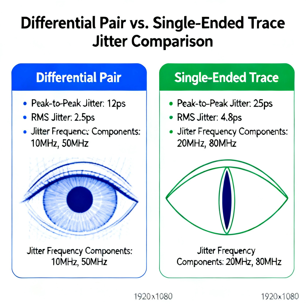
Head-to-Head Comparison – Differential vs. Single-Ended Jitter Performance in High Speed PCB
| Parameter | Single-Ended | Differential | Why It Matters |
|---|---|---|---|
| Ground Bounce (SSN) Rejection | Poor | Excellent | Differential signals are immune to ground reference shifts. |
| Power Supply Noise Rejection | Poor | Excellent | PSRR of differential receivers is very high. |
| Crosstalk Susceptibility | High | Low | Magnetic field cancellation reduces aggressor coupling. |
| ISI (DDJ) Sensitivity | Moderate | Low | Tight impedance control is easier with differential pairs. |
| Skew-Induced Jitter | Not applicable | Critical (intra-pair) | Single-ended signals have no pair skew. |
| EMI Emission | High | Low | Differential pairs radiate less. |
| Jitter Budget for 10 Gbps | ~10-20 ps pk-pk | ~5-10 ps pk-pk | Differential signaling allows higher data rates. |
Critical Insight from Johnson & Graham: “The single most effective way to reduce jitter in a high-speed system is to use differential signaling wherever possible. The cost in board area and routing complexity is almost always worth the improvement in timing margin.”
Practical PCB Design Rules to Minimize Jitter in High Speed PCB
Based on the top three sources, here is a consolidated set of actionable rules: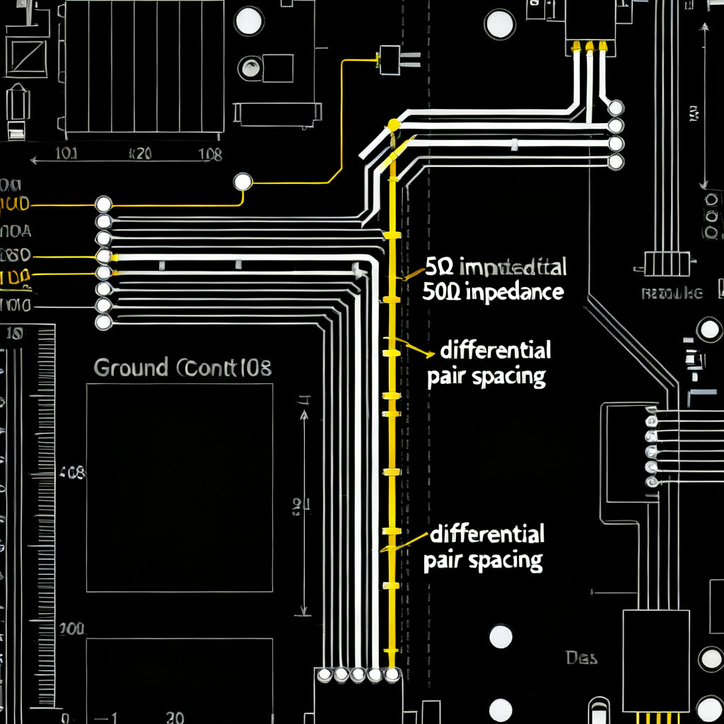
For Single-Ended Traces (When You Must Use Them)
- Return Path Integrity: Never route a single-ended trace over a split in the ground plane. Use a solid, continuous reference plane.
- Decoupling: Use a 0.1µF + 1µF + 10µF capacitor network per power pin. Place the smallest capacitor closest to the pin.
- Length Matching: Match trace lengths within 10% of the rise time (e.g., for a 100ps rise time, match within 10ps).
- Termination: Use series termination (Rs) at the source to match the driver impedance to the trace impedance. This eliminates reflections that cause ISI.
For Differential Pairs (The Preferred Method)
- Intra-Pair Skew: Match the P and N traces to within 1-2 mils of total length. Use serpentine bends only on the shorter trace, and keep the bend radius > 3x the trace width.
- Inter-Pair Skew: Match all differential pairs in a bus (e.g., PCIe lane pairs) to within 5-10 ps.
- Coupling: Keep the differential pair tightly coupled (edge-to-edge spacing = 2x trace width) to maximize common-mode rejection. Do not separate the traces around vias or pads.
- Vias: Minimize the number of vias per pair. Each via adds ~5-10 ps of jitter due to impedance discontinuity. Use back-drilling to remove unused via stubs.
- Grounding: Provide a ground via near every differential via to provide a return path for any common-mode current.
Stack-Up Recommendations for Jitter Reduction
- For Differential Signals: Use a stripline layer (between two ground planes) for the best isolation. The ground planes act as shields, reducing crosstalk by 20-30 dB.
- For Single-Ended Signals: Use microstrip on the outer layers, with a solid ground plane on the adjacent layer. Avoid routing single-ended signals on inner layers without a reference plane.
How to Specify Jitter Requirements for Your High Speed PCB Manufacturer
When ordering high-speed PCBs from us, you must clearly specify jitter-related parameters. Here is a checklist:
- Impedance Tolerance: Specify Zdiff (e.g., 100Ω ±5%) and Zo (e.g., 50Ω ±5%).
- Skew Tolerance: Specify maximum intra-pair skew (e.g., < 2 ps).
- Dielectric Material: Specify low-loss materials (e.g., Rogers 4350B or Isola FR408) for frequencies > 5 GHz.
- Surface Finish: Specify ENIG (Electroless Nickel Immersion Gold) for better high-frequency performance than HASL.
- Back-Drilling: Specify back-drilling for all via stubs on differential pairs.
Why This Matters: A poorly manufactured PCB can add 10-20 ps of jitter from impedance mismatches and via stubs alone, even if your design is perfect. Partnering with an experienced B2B manufacturer ensures your jitter budget is preserved.
Conclusion: The Verdict for High-Speed Design in High Speed PCB
For any high-speed design operating above 1 Gbps, differential signaling is the clear winner for jitter performance. It provides inherent immunity to ground bounce, power supply noise, and crosstalk—the three largest sources of deterministic jitter. Single-ended signaling, while simpler and cheaper, is fundamentally limited by these noise sources.
However, even differential pairs are not immune to jitter. Intra-pair skew, impedance mismatch, and via discontinuities are the new enemies. By understanding the physics of jitter in both topologies, and by applying the rigorous layout rules outlined in this pillar page, you can design PCBs that achieve the lowest possible bit error rates.
Next Steps for Your Project:
- [ ] Review your current design for differential pair skew.
- [ ] Specify impedance tolerance and material requirements in your next PCB order.
- [ ] Contact our engineering team for a free signal integrity review of your layout.
Related Content:
- How to Calculate Differential Impedance for Your Stack-Up
- The Ultimate Guide to Crosstalk Mitigation in PCB Layout
- Back-Drilling: The Secret to 40 Gbps PCB Performance