In high-speed PCB design, the eye diagram is the single most powerful diagnostic tool for evaluating signal quality. It provides a visual representation of a digital signal’s health over time, revealing issues like jitter, noise, crosstalk, and impedance mismatches. For B2B PCB manufacturers and engineers working with High-Speed designs—whether for differential pairs (e.g., USB, HDMI, PCIe) or single-ended lines (e.g., DDR memory, SPI, I2C)—mastering the eye diagram is essential for ensuring first-pass success and reliable performance.
This Pillar Content page synthesizes the most authoritative knowledge from industry-leading sources (Altium, Cadence, and Sierra Circuits) to deliver a complete, no-fluff guide. We will cover:
- What an eye diagram is and how it is constructed.
- The critical differences between differential and single-ended eye diagrams.
- Key parameters to analyze (jitter, eye height, eye width, eye opening, mask margins).
- How to optimize your PCB stackup, routing, and termination for both signal types.
- Common pitfalls and best practices for achieving a clean eye.
Part 1: What Is an Eye Diagram? The Fundamental Concept
1.1 Construction of the Eye Diagram
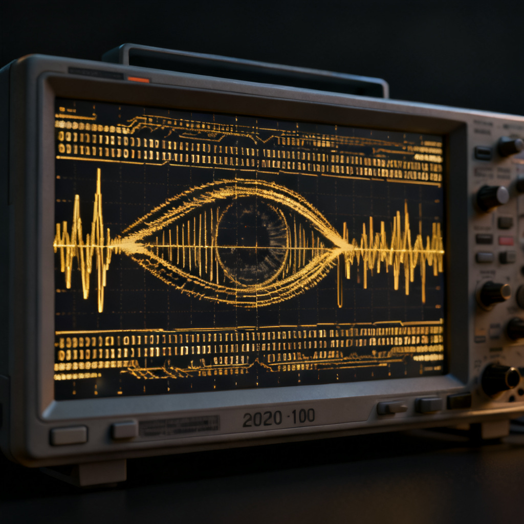
An eye diagram is created by overlaying many successive bits of a digital signal on an oscilloscope, triggered by a clock or a data pattern. The oscilloscope’s persistence mode captures the transitions from low to high (rising edges) and high to low (falling edges), superimposing them to form an “eye” shape.
Key components of the eye diagram:
- Eye Opening: The clear area in the center of the diagram. A larger opening indicates better signal quality.
- Eye Height: The vertical opening, representing the voltage margin between logic high (1) and logic low (0). It is affected by noise, attenuation, and impedance mismatches.
- Eye Width: The horizontal opening, representing the time margin for sampling. It is affected by jitter (timing uncertainty) and deterministic effects like intersymbol interference (ISI).
- Rise Time and Fall Time: The slopes of the transitions. Slower rise/fall times can close the eye but reduce EMI; excessively fast times can cause overshoot and ringing.
- Jitter: The horizontal displacement of edges from their ideal position. Jitter is categorized as random (Gaussian) or deterministic (data-dependent, periodic, bounded).
- Noise: The vertical displacement of the signal levels, often caused by power supply noise, crosstalk, or ground bounce.
1.2 Why the Eye Diagram Matters for High-Speed PCB Design
For B2B PCB fabrication and assembly, the eye diagram is the ultimate pass/fail criteria. A closed eye (no clear opening) means the receiver cannot distinguish a 1 from a 0, leading to bit errors. Key reasons to analyze eye diagrams:
- Validate Design Rules: Ensure trace widths, spacing, stackup, and via structures meet signal integrity requirements.
- Identify Impedance Discontinuities: Reflections from connectors, vias, or mismatched terminations show as eye closure.
- Quantify Jitter Budget: Verify that total jitter (Tj) stays within the receiver’s tolerance.
- Optimize Pre-Emphasis/Equalization: Adjust driver settings to compensate for channel losses.
- Compliance Testing: Many high-speed standards (USB 3.0, PCIe Gen 4, HDMI 2.0) mandate specific eye mask templates.
Part 2: Eye Diagram for Single-Ended Signals
2.1 Characteristics of Single-Ended Signals
Single-ended signals transmit data on one conductor, referenced to a common ground (GND). Examples include CMOS, TTL, SPI, I2C, and DDR memory address/control lines. They are simpler to route but more susceptible to noise and crosstalk.
Eye diagram behavior for single-ended:
- The eye is defined by the voltage swing between VOH (output high) and VOL (output low).
- Ground bounce and simultaneous switching noise (SSN) cause vertical eye closure.
- Crosstalk from adjacent traces (especially in parallel buses) introduces noise that narrows the eye height.
- Reflections from open stubs or unterminated lines cause ringing and overshoot, degrading the eye width.
2.2 Key Parameters for Single-Ended Eye Analysis
- Eye Height (Veye): The minimum voltage difference between logic levels at the sampling point. For standard 3.3V CMOS, a healthy eye might be 2.5V; for 1.8V DDR, it might be 1.0V.
- Eye Width (Teye): The time window where the signal is stable. Jitter from clock sources or data-dependent effects (e.g., ISI) reduces this.
- Rise/Fall Time Degradation: Long traces or high capacitance loads slow down edges, closing the eye.
- Overshoot and Undershoot: Excessive ringing can violate receiver absolute maximum ratings, causing long-term reliability issues.
- Mask Margin: A compliance mask (e.g., from the JEDEC standard for DDR) defines a forbidden zone. The signal must not enter this zone.
2.3 Design Best Practices for Single-Ended Signals
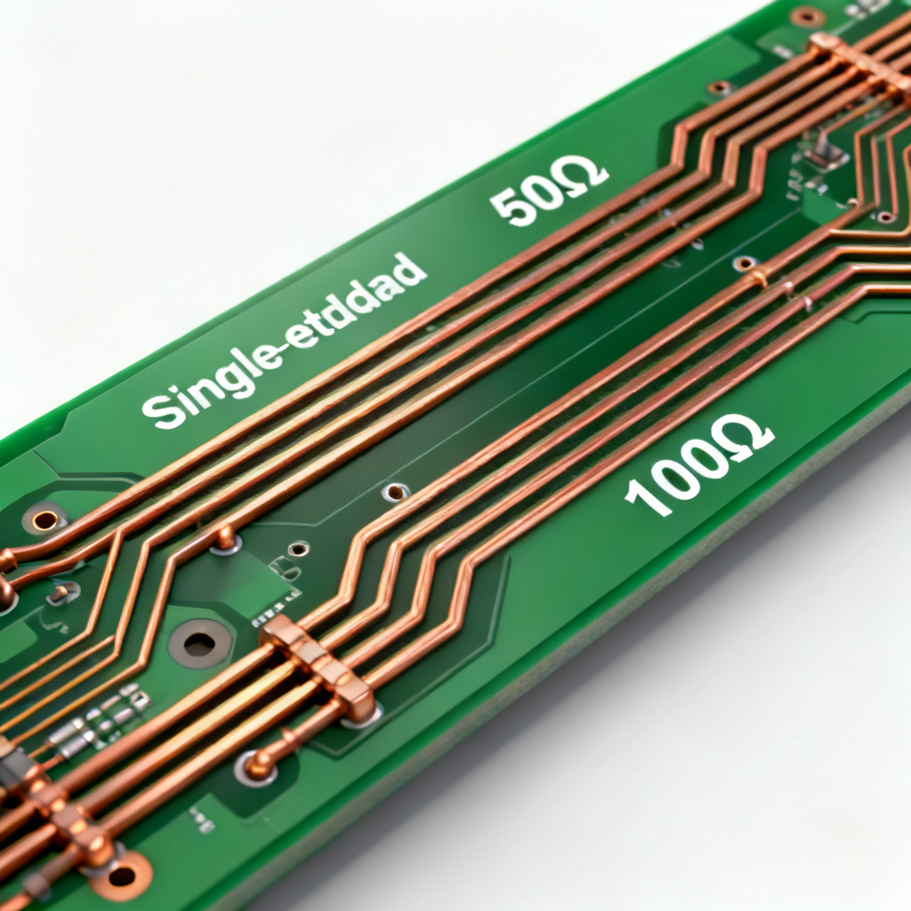
- Impedance Control: Match the trace impedance (e.g., 50Ω single-ended) to the driver and receiver. Use controlled impedance stackups with proper dielectric materials (e.g., FR4, Rogers, or Isola).
- Termination: Series termination (resistor near the driver) or parallel termination (resistor to VCC/GND at the receiver) reduces reflections. For point-to-point lines, series termination is common.
- Ground Planes: Provide a continuous, low-inductance return path. Avoid splits in the ground plane under high-speed traces.
- Spacing: Maintain at least 3x the trace width (3W rule) to minimize crosstalk. For parallel buses (e.g., DDR data lines), use 5W or more.
- Length Matching: For multi-bit buses, match trace lengths to within a few ps to avoid skew-induced eye closure.
- Avoid Stubs: Keep stubs as short as possible (ideally < 1/10th of the signal rise time length). Use daisy-chain or fly-by routing for DDR topologies.
Part 3: Eye Diagram for Differential Signals
3.1 Characteristics of Differential Signals
Differential signals use two complementary traces (P and N) to transmit data, with the receiver sensing the voltage difference between them. Examples include USB, Ethernet, HDMI, PCIe, LVDS, and SATA.
Eye diagram behavior for differential:
- The eye is plotted as the differential voltage (Vdiff = V(P) – V(N)).
- Common-mode noise (from power supply or EMI) is rejected, resulting in a cleaner eye.
- The differential impedance (Zdiff) must be controlled (e.g., 100Ω for USB, 90Ω for PCIe).
- Skew between the P and N traces (intentional or unintentional) converts common-mode noise to differential noise, closing the eye.
3.2 Key Parameters for Differential Eye Analysis
- Differential Eye Height: The voltage margin of the differential signal. It is typically larger than single-ended eye height for the same swing because of the 2x voltage difference.
- Differential Eye Width: The time margin, influenced by differential jitter. Common-mode jitter is less impactful.
- Common-Mode Voltage (Vcm): The average of P and N. Ideally constant; variations indicate imbalance.
- Intra-Pair Skew: The time delta between P and N transitions. Even 1 ps of skew can degrade high-speed signals (e.g., 10 Gbps+).
- Mode Conversion: SCD21 (single-ended to differential) and SDC21 (differential to common-mode) parameters indicate how well the pair is balanced. Poor balance increases EMI and eye closure.
- Differential Insertion Loss (SDD21): The attenuation of the differential signal. Excessive loss closes the eye vertically.
3.3 Design Best Practices for Differential Signals
- Differential Impedance Control: Use a stackup that provides the target Zdiff (e.g., 100Ω). Typical trace widths and spacing: 5 mil trace, 5 mil gap (edge-coupled) or broadside-coupled.
- Symmetry: Keep P and N traces identical in length, width, and proximity to other structures. Avoid bends that introduce skew (use 45° or arc bends, not 90°).
- Length Matching: Match intra-pair lengths to within 5 mils (or 1 ps). For multi-lane interfaces (e.g., PCIe), match inter-pair lengths as well.
- Grounding: Provide a continuous ground plane beneath the differential pair. Do not route over splits. Add ground vias near connector transitions.
- AC Coupling Capacitors: For many standards (e.g., PCIe, USB 3.0), use series capacitors (typically 0.1 µF) to block DC bias. Place them symmetrically (same distance from driver) to avoid skew.
- Via Optimization: Use ground vias adjacent to signal vias to provide a return path and reduce impedance discontinuity. Back-drill unused via stubs for high-speed signals (>10 Gbps).
- Termination: Use a single termination resistor (Rterm) across the receiver inputs, matching Zdiff. For LVDS, this is typically 100Ω.
Part 4: Head-to-Head Comparison: Differential vs Single-Ended Eye Diagrams
| Parameter | Single-Ended Eye | Differential Eye |
|---|---|---|
| Voltage Swing | VOH – VOL (e.g., 3.3V, 1.8V) | 2x the single-ended swing (e.g., 0.35V for LVDS) |
| Noise Immunity | Low (susceptible to ground bounce, crosstalk) | High (common-mode rejection) |
| Jitter Sources | Power noise, crosstalk, ISI | Intra-pair skew, mode conversion, common-mode noise |
| Eye Opening | Smaller for same swing due to noise | Larger for same power due to differential nature |
| Routing Complexity | Simple (single trace) | More complex (requires matched pair) |
| EMI Susceptibility | High | Low (fields cancel) |
| Common Applications | DDR, SPI, I2C, CMOS logic | USB, HDMI, PCIe, Ethernet, SATA |
| Impedance Target | 50Ω (typical) | 100Ω or 90Ω (typical) |
| Termination | Series or parallel to GND/VCC | Single resistor across pair |
Why differential often wins for high-speed:
- Lower voltage swing reduces power consumption and EMI.
- Inherent noise rejection allows longer trace lengths and higher data rates.
- Eye closure is dominated by skew, which is easier to control than single-ended noise.
When single-ended is still preferred:
- Lower cost (fewer layers, simpler routing).
- Wider availability of standard logic families.
- For parallel buses (e.g., DDR4/5) where differential is not feasible for all lines.
Part 5: How to Measure and Improve Your Eye Diagram
5.1 Measurement Techniques
- Real-Time Oscilloscope (DSO): Used for capturing long data sequences (e.g., PRBS patterns). Provides jitter decomposition and statistical analysis.
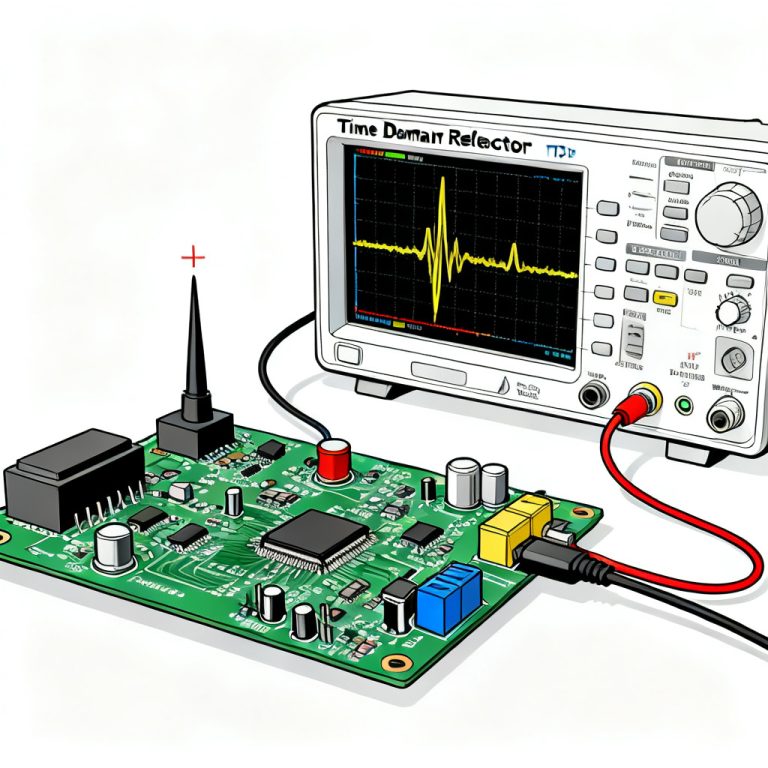
- Sampling Oscilloscope (TDR/TDT): Used for high-bandwidth measurements (up to 100 GHz). Ideal for differential signals and impedance characterization.
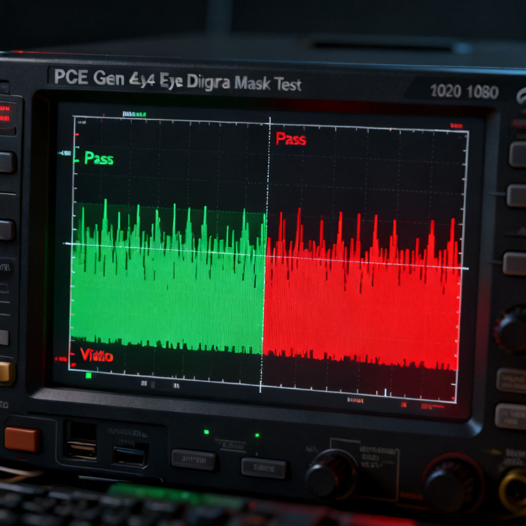
- Eye Mask Testing: Automatically compares the eye against a predefined mask. Pass/fail criteria are standard for compliance.
Key measurement settings:
- Bit Rate: Set to the operating data rate (e.g., 5 Gbps for USB 3.0).
- Pattern Length: Use a PRBS7 or PRBS31 pattern to stress the channel.
- Trigger Source: Use the clock or a recovered clock from the data.
- Number of Bits: Capture at least 1 million bits for statistical validity.
5.2 Common Root Causes of a Closed Eye
| Symptom | Likely Cause | Fix |
|---|---|---|
| Narrow eye width (horizontal) | Jitter (random or deterministic) | Improve clock jitter, reduce crosstalk, match lengths |
| Low eye height (vertical) | Attenuation, noise, or poor term | Increase driver strength, use pre-emphasis, improve impedance |
| Overshoot/ringing | Impedance mismatch | Add termination, reduce stub lengths |
| Asymmetric eye (differential) | Intra-pair skew | Match trace lengths, check via symmetry |
| Double-edge (multiple transitions) | Reflections from unterminated line | Add termination at receiver |
| Noise floor rising | Power supply noise or crosstalk | Improve decoupling, increase spacing |
5.3 PCB Optimization Checklist (For Your B2B Manufacturing)
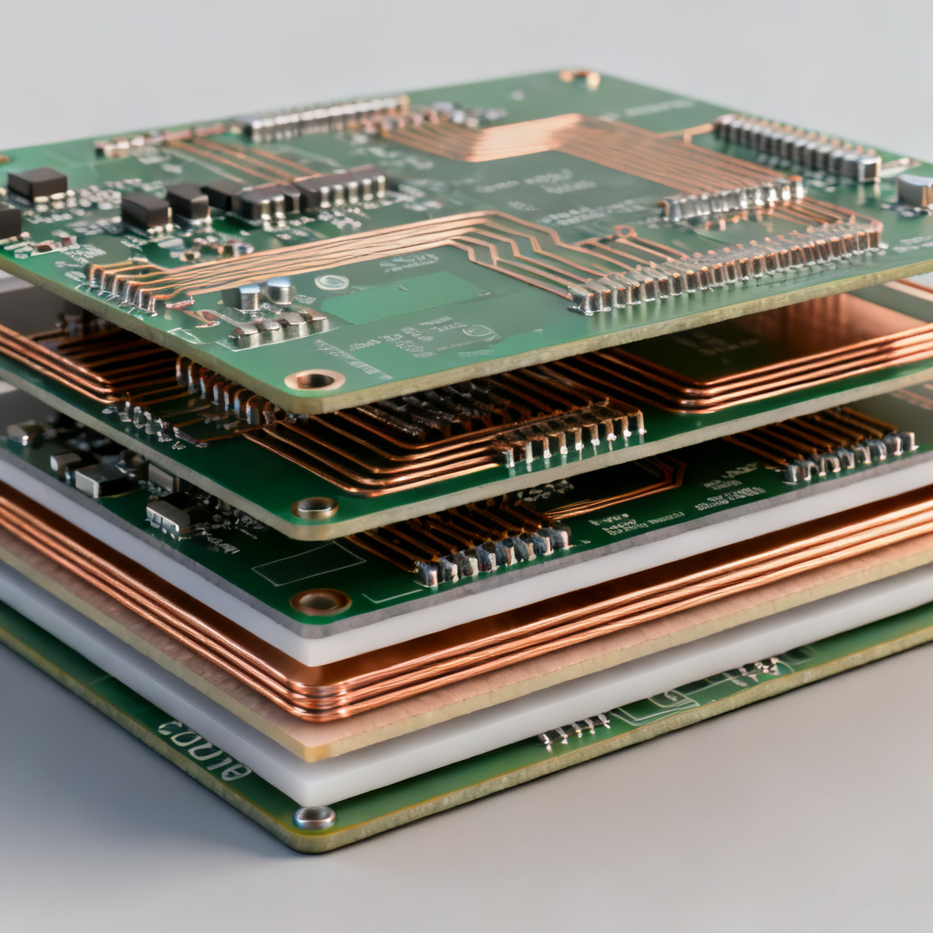
- Stackup Design:
- Use at least 4 layers for high-speed signals (signal, GND, power, signal).
- Place high-speed signals adjacent to a solid ground plane.
- Choose low-loss dielectric (e.g., FR4 with low Df, or Rogers for >10 Gbps).
- Trace Geometry:
- Calculate impedance using field solvers (e.g., Polar SI9000).
- For differential pairs, use edge-coupled microstrip or stripline.
- Maintain constant trace width and spacing; avoid neck-downs.
- Via Management:
- Minimize via count per signal path.
- Use back-drilling for vias > 1 Gbps.
- Add ground stitching vias near differential pair vias.
- Component Placement:
- Keep high-speed drivers close to connectors.
- Place termination resistors as close to the receiver as possible.
- Use AC coupling caps with low ESL (e.g., 0402 or 0201 packages).
- Manufacturing Tolerances:
- Specify ±10% impedance tolerance (tighter for >10 Gbps).
- Request controlled etching and dielectric thickness verification.
- Use impedance coupon testing on every panel.
Part 6: Real-World Examples and Case Studies
Example 1: Single-Ended DDR4 Data Line
Symptom: Eye height at receiver was only 0.6V (spec requires >0.8V). Root Cause: Long trace (8 inches) with high capacitance from multiple DIMM slots, plus 50Ω impedance mismatch (actual Z0 = 45Ω). Fix: Changed stackup to achieve 50Ω, reduced trace length to 6 inches, added series termination (22Ω) near the driver. Result: Eye height increased to 1.1V.
Example 2: Differential PCIe Gen 3 (8 Gbps)
Symptom: Eye mask violation at the center of the eye. Root Cause: Intra-pair skew of 3 ps due to a 45° bend on one trace (P) and a 90° bend on the other (N). Fix: Re-routed both traces with identical 45° bends and matched lengths to within 2 mils. Result: Eye passed mask with 20% margin.
Example 3: Single-Ended vs Differential for a 5 Gbps Link
- Single-ended attempt: Required 1.2V swing, 50Ω impedance, careful decoupling. Eye height was 0.9V, width 120 ps (jitter = 20 ps). Marginal.
- Differential alternative (LVDS): 350 mV swing, 100Ω impedance. Eye height was 0.6V (differential), width 150 ps (jitter = 10 ps). Result: Robust performance with lower power.
Part 7: Conclusion and Next Steps for Your High-Speed PCB Design
The eye diagram is not just a test tool—it is a design philosophy. Whether you are routing single-ended DDR4 or differential PCIe Gen 5, the principles remain the same:
- Control impedance.
- Minimize discontinuities.
- Match lengths.
- Provide clean power and ground.
For B2B PCB manufacturers and OEMs, investing in eye diagram analysis during the design phase saves weeks of re-spins and millions in scrap. By understanding the nuances between differential and single-ended signals, you can make informed decisions about stackup, routing, and termination.
Ready to produce your High-Speed PCB? Contact our engineering team for a free design review. We specialize in controlled impedance PCBs with ±5% tolerance, back-drilling, and advanced material options. Upload your Gerber files today for a quick quotation.
FAQ: Eye Diagram PCB for Differential vs Single-Ended Signals
What is an eye diagram in PCB design?
An eye diagram PCB is a visual representation of a digital signal’s health over time, created by overlaying multiple bit transitions on an oscilloscope. It reveals jitter, noise, and impedance issues critical for high-speed signal integrity.
How does the eye diagram differ for differential vs single-ended signals?
For single-ended signals, the eye diagram PCB shows voltage swing between VOH and VOL, often degraded by ground bounce and crosstalk. For differential signals, the eye is based on Vdiff, offering better noise immunity and a larger opening due to common-mode rejection, though it is sensitive to intra-pair skew.
What are the key parameters to analyze in an eye diagram?
Key parameters include eye height (voltage margin), eye width (time margin), jitter (timing uncertainty), rise/fall times, and mask margin. For differential signals, also monitor common-mode voltage and intra-pair skew.
How can I improve the eye diagram for my high-speed PCB?
Improve the eye diagram PCB by controlling impedance (e.g., 50Ω single-ended, 100Ω differential), matching trace lengths, minimizing stubs, using proper termination, and optimizing via structures. For differential pairs, ensure symmetry and avoid skew.