In modern PCB design, the return path PCB design for high current vs high speed signals presents a fundamental conflict that directly impacts signal integrity and power delivery. This guide synthesizes insights from top industry sources to help B2B engineers balance these opposing needs for optimal high-speed PCB performance.
Understanding the Return Path for High Speed vs High Current
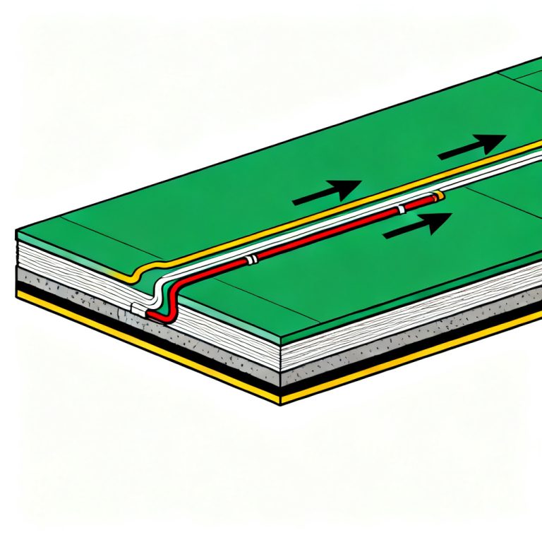
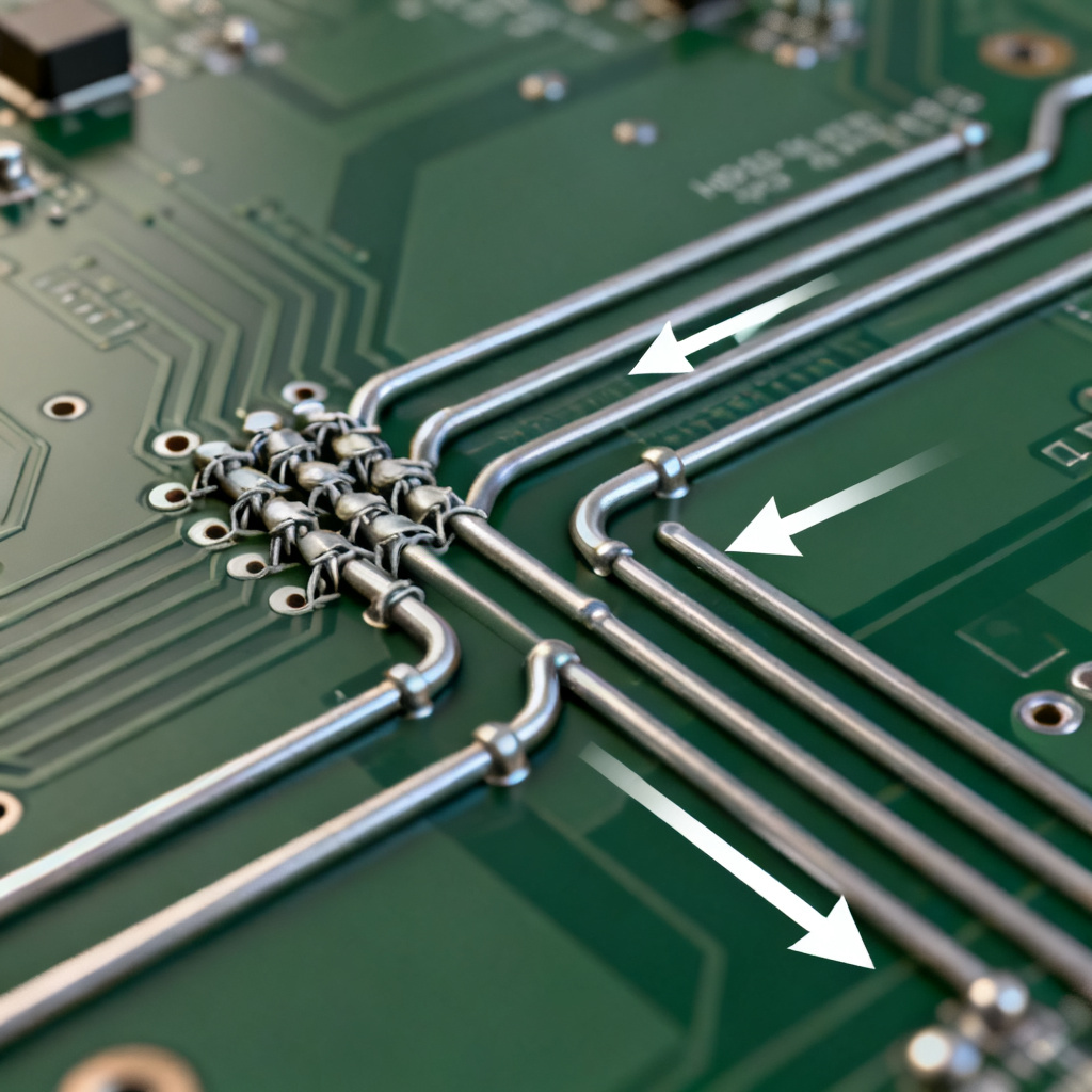
The return path PCB design for high current vs high speed signals begins with recognizing that high-speed signals demand a continuous, low-inductance ground plane, while high-current paths require wide, low-resistance copper areas. For high-speed signals, the return path must be a solid reference plane directly adjacent to the signal trace to minimize loop area and EMI. For high-current paths, the return path must be wide and thick to handle current without excessive voltage drop or heat generation. The conflict arises because high-speed signals need an uninterrupted ground plane, while high-current paths often introduce slots or breaks in that same plane for isolation or thermal management.
Impedance vs. Resistance in Return Path Design
High-speed signals require controlled impedance (e.g., 50Ω), achieved through a precise dielectric thickness and continuous return plane. High-current paths prioritize low DC resistance (DCR), demanding wide copper pours that can alter impedance. A wide, high-current copper pour under a high-speed trace lowers impedance, causing mismatch and reflections.
Inductance and Loop Area Trade-offs
High-speed signals need minimal loop area with return current flowing directly beneath the trace. High-current paths require wide return paths to spread current and reduce magnetic fields, conflicting with the tight geometry needed for low inductance.
Ground Plane Integrity Challenges
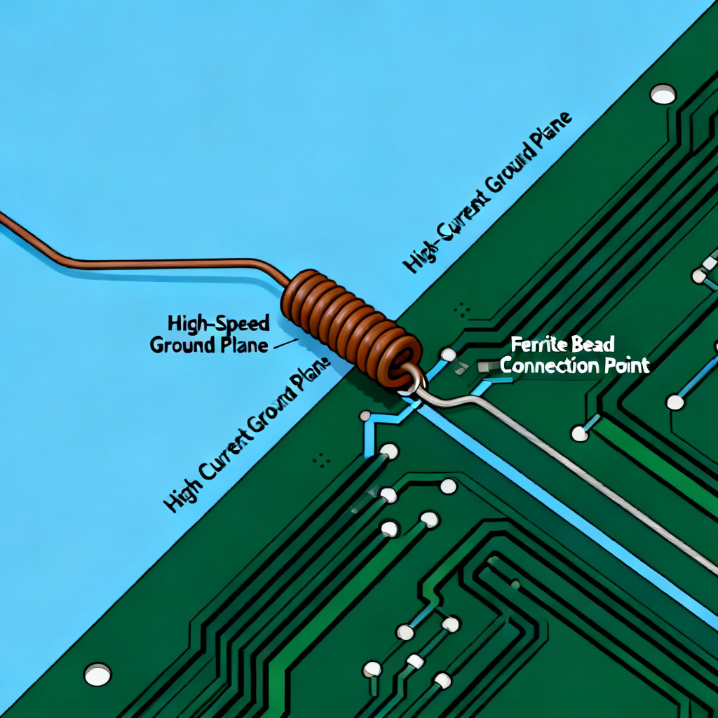
A solid ground plane is non-negotiable for high-speed signals, yet high-current paths often require slots or cutouts for isolation. The solution involves separate ground planes connected at a single point (star grounding) or via ferrite beads.
Conflicting Requirements Analysis: Return Path PCB Design
The return path PCB design for high current vs high speed signals involves three core conflicts: impedance vs. resistance, inductance vs. loop area, and ground plane integrity. Each conflict requires a strategic approach to resolve without compromising performance.
Impedance Control vs. Low Resistance
High-speed signals rely on controlled impedance (50Ω or 100Ω differential), while high-current paths demand low DCR. A wide copper pour under a high-speed trace reduces impedance, while a narrow return path cannot handle high current.
Minimizing Inductance vs. Spreading Current
High-speed signals require tight loop area for low inductance, but high-current paths need wide return paths to spread current and reduce magnetic field concentration.
Solid Ground Plane vs. Isolation Slots
High-speed signals need uninterrupted ground planes, but high-current paths often require slots to isolate noisy circuits. Star grounding or ferrite beads can bridge these needs.
Resolving the Conflict: Practical Strategies for Return Path PCB Design
To address return path PCB design for high current vs high speed signals, implement these proven strategies from industry experts.
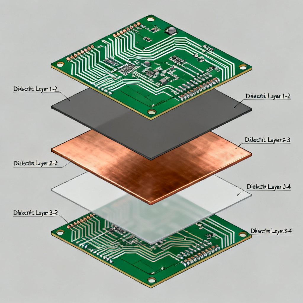
Layer Stackup Optimization
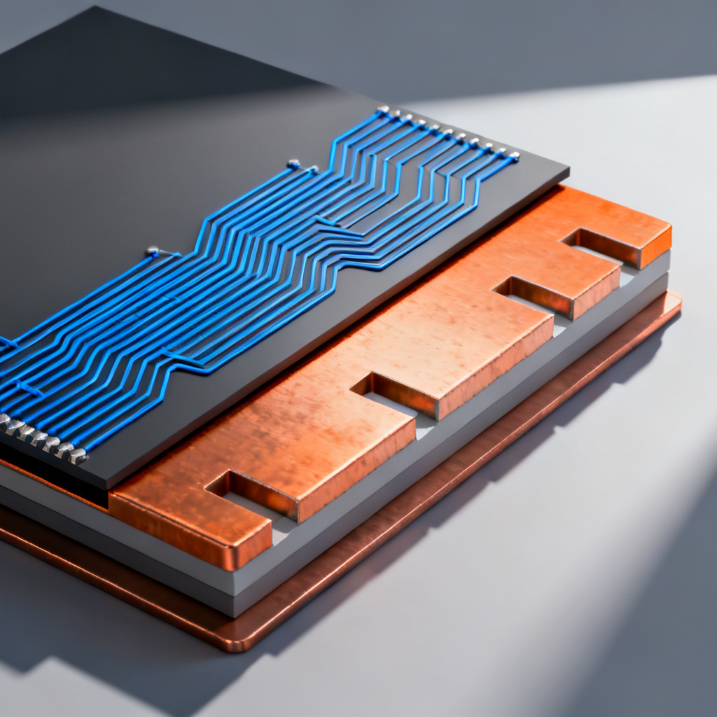
Use a multi-layer stackup with dedicated layers: Layer 2 as a solid ground plane for high-speed return, and Layer 3 as a power plane with wide copper pours for high-current distribution. This physically separates conflicting return paths.
Via Stitching and Multiple Vias
For high-speed signals, use multiple via stitches (3-4 per transition) near signal vias to maintain low inductance. For high-current paths, use multiple vias in parallel to reduce resistance and current density.
Star Grounding and Island Grounding
Implement star grounding where all ground planes meet at a single point to prevent ground loops. Use ferrite beads or zero-ohm resistors to connect separate ground islands for high-current circuits.
Current Return Path Routing
Treat high-current return paths as dedicated traces with wide, short routes and multiple vias. For high-speed signals, ensure the return path is directly beneath the trace. Use ground plane bridges for crossings.
Thermal Management for High Current
High-current paths generate heat; use thermal vias under components to transfer heat to internal copper planes. Place these vias away from high-speed traces to avoid disrupting the return path.
Case Studies: Real-World Return Path PCB Design Examples
These case studies illustrate how return path PCB design for high current vs high speed signals is resolved in practice.
High-Speed Digital with Power Distribution
Scenario: A 10-layer PCB with 1 Gbps DDR4 bus (high-speed) and 20A FPGA power supply (high-current). Problem: High-current return path on the same ground plane as DDR4 signals caused noise coupling. Solution: Layer 2 solid ground plane for DDR4; Layer 5 power plane for 20A return connected at single point; via stitching near DDR4 vias. Result: Signal integrity improved by 15 dB; power delivery efficiency increased by 8%.
High-Current Motor Driver with High-Speed Communication
Scenario: A 4-layer PCB for robotic arm with 30A motor driver (high-current) and 100 Mbps CAN bus (high-speed). Problem: Motor driver return path created magnetic field inducing noise on CAN bus. Solution: Isolated motor driver ground plane (Layer 4) from CAN bus ground plane (Layer 2) via 1 mm slot; connected at single point with ferrite bead; CAN bus routed over solid ground plane. Result: EMI reduced by 20 dB; CAN bus error rate zero.
Best Practices for B2B PCB Manufacturing
For return path PCB design for high current vs high speed signals, partner with a manufacturer offering advanced stackup options (4-20 layers, controlled impedance, thick copper up to 3 oz), via technology (microvias, buried vias, via-in-pad), low-loss materials (Rogers 4350B), and testing (impedance testing, IR thermal imaging).
| Parameter | High-Speed Signal Requirement | High-Current Path Requirement |
|---|---|---|
| Return Path Type | Solid ground plane | Wide copper pour |
| Impedance Target | 50Ω or 100Ω differential | Low DCR (<10 mΩ) |
| Copper Thickness | 1 oz typical | 2-3 oz |
| Via Strategy | Stitching near signal vias | Multiple parallel vias |
| Ground Plane Integrity | Uninterrupted | Isolation slots allowed |
Frequently Asked Questions about Return Path PCB Design
What is the main conflict in return path PCB design for high current vs high speed signals?
The main conflict is that high-speed signals require a continuous, low-inductance ground plane, while high-current paths need wide, low-resistance copper areas that may introduce slots or breaks in that plane. This return path PCB design for high current vs high speed signals conflict must be resolved through layer stackup optimization and star grounding.
How can I resolve the conflicting requirements of return path design?
Resolve conflicts by using multi-layer stackups with separate ground planes for high-speed and high-current paths, implementing via stitching for high-speed signals, multiple vias for high-current paths, and star grounding to connect ground islands. These strategies balance return path PCB design for high current vs high speed signals effectively.
Why is ground plane integrity important for high-speed signals?
A solid ground plane provides a low-inductance return path, minimizing loop area, signal reflections, and EMI. Any slot or break in the ground plane under a high-speed trace disrupts the return path PCB design for high current vs high speed signals, causing signal integrity degradation.
What materials are best for high-speed and high-current PCBs?
For high-speed signals, use low-loss materials like Rogers 4350B. For high-current paths, use FR4 with high Tg for thermal performance. The return path PCB design for high current vs high speed signals benefits from combining these materials in a hybrid stackup.
Can I use the same ground plane for both high-speed and high-current signals?
It is not recommended because high-current return paths introduce noise and voltage drops that affect high-speed signal integrity. Use separate ground planes connected at a single point (star grounding) to manage return path PCB design for high current vs high speed signals.