Learn how to set up crosstalk simulation in high speed PCB using HyperLynx for pre-layout and post-layout analysis. This guide covers fundamentals, step-by-step workflows, and expert mitigation strategies to ensure signal integrity in your high-speed designs.
1. Understanding Crosstalk Fundamentals Before Simulation
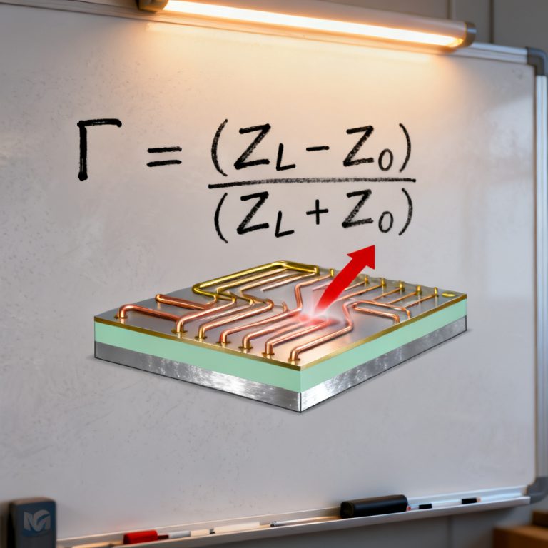
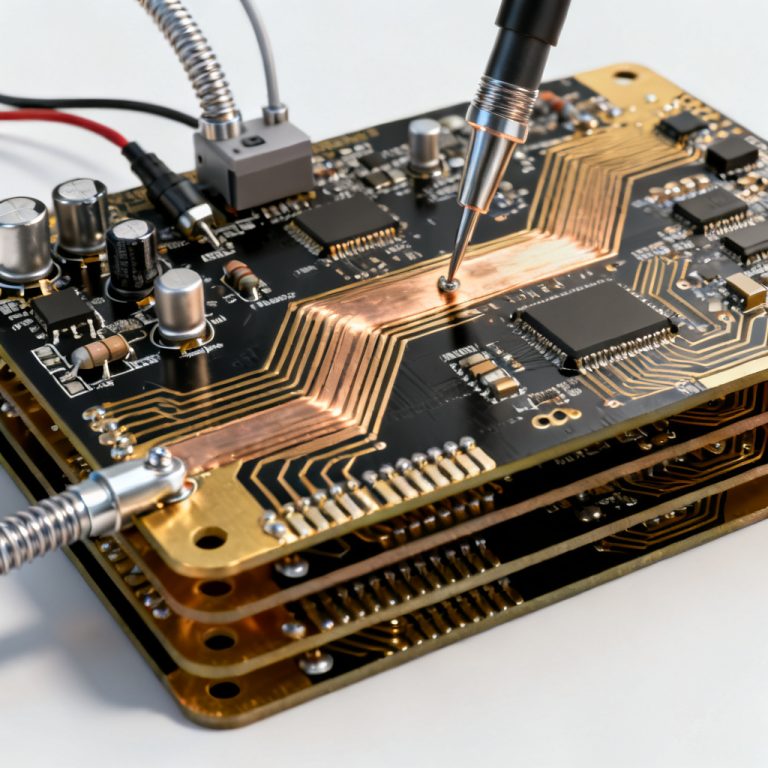
Crosstalk simulation in high speed PCB begins with understanding electromagnetic coupling. Crosstalk occurs through capacitive and inductive coupling, with inductive coupling dominating for fast edge rates below 1 ns. Key parameters include dielectric constant (Dk), trace spacing (S), height above reference plane (H), edge rate, parallel coupling length, and termination impedance. HyperLynx models forward and backward crosstalk, with backward crosstalk typically larger in microstrip traces due to inhomogeneous dielectric.
1.1 Key Parameters Influencing Crosstalk
Crosstalk simulation in high speed PCB requires careful control of these parameters: Dk reduces capacitive coupling; the 3W rule (S ≥ 3× trace width) is a starting point; faster edges generate higher harmonics; longer parallel runs increase coupled energy; mismatched terminations cause reflections. HyperLynx models forward and backward crosstalk, with backward crosstalk typically larger in microstrip traces due to inhomogeneous dielectric.
1.2 Coupling Mechanisms
Crosstalk simulation in high speed PCB distinguishes between capacitive (electric field) and inductive (magnetic field) coupling. Inductive coupling dominates for fast edge rates (<1 ns). HyperLynx models both as forward crosstalk (far end) and backward crosstalk (near end).
2. Pre-Layout Crosstalk Simulation in HyperLynx: The “What-If” Analysis
Pre-layout crosstalk simulation in high speed PCB using HyperLynx LineSim allows exploration of trade-offs before layout commitment.
2.1 Launch LineSim and Define the Stackup
Crosstalk simulation in high speed PCB starts with accurate stackup definition. In LineSim, go to Stackup Editor to define layer count, material properties (e.g., FR4 with Dk=4.2 at 1 GHz, loss tangent=0.02), copper thickness (e.g., 1 oz = 1.4 mils), and dielectric thickness (e.g., 4 mils for microstrip). Even a 10% error in dielectric thickness can shift predictions by 20–30%.
2.2 Create the Coupled Trace Model
Crosstalk simulation in high speed PCB requires placing aggressor and victim traces on the same layer. Set trace width (e.g., 5 mils for 50-ohm impedance), length (e.g., 2 inches), and spacing (e.g., 5, 10, 15 mils). Use the Coupled Trace Wizard to generate multiple coupled segments for parametric sweeps.
2.3 Assign Drivers and Terminations
Crosstalk simulation in high speed PCB uses digital drivers (e.g., 3.3V LVCMOS with 100 ps rise time) on the aggressor and passive terminations (e.g., 50-ohm resistor to ground) at the far end. For the victim, leave both ends open (worst-case) or add 50-ohm terminations. Use IBIS models for realistic output impedance and slew rate.
2.4 Run the Crosstalk Simulation
Crosstalk simulation in high speed PCB is performed via Simulate → Crosstalk. Select aggressor and victim nets, choose Time Domain (waveform viewing) or Frequency Domain (S-parameters), set simulation time (e.g., 10 ns) and step size (e.g., 1 ps), then click Run.
2.5 Interpret the Results
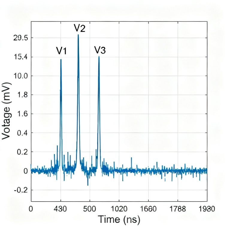
Crosstalk simulation in high speed PCB results show near-end crosstalk (NEXT) and far-end crosstalk (FEXT). For microstrip traces, NEXT is typically larger. If peak crosstalk exceeds 10% of the victim’s logic swing (e.g., 330 mV for 3.3V), adjust spacing or stackup.

3. Post-Layout Crosstalk Simulation in HyperLynx: Validating the Real Board
Post-layout crosstalk simulation in high speed PCB using HyperLynx BoardSim validates actual routed traces.
3.1 Import the PCB Layout
Crosstalk simulation in high speed PCB imports board files (.brd, .pcb, .hyp) into BoardSim. HyperLynx automatically extracts stackup, net topology, and via structures.
3.2 Select the Aggressor-Victim Pair
Crosstalk simulation in high speed PCB uses the Net Browser to select high-speed nets (e.g., DDR clock line) as aggressors. Use the Crosstalk Wizard to automatically detect potential victims within a user-defined spacing threshold (e.g., 10 mils). Pay attention to parallel runs on adjacent layers (broadside coupling).
3.3 Configure the Simulation
Crosstalk simulation in high speed PCB assigns IBIS models to all IC pins. If unavailable, use generic driver models (e.g., 50-ohm output impedance, 200 ps rise time). Set simulation bandwidth to at least 5× the highest frequency (e.g., 5 GHz for 1 GHz clock). Enable crosstalk coupling in simulation settings.
3.4 Run Post-Layout Crosstalk Simulation
Crosstalk simulation in high speed PCB is executed via Simulate → Crosstalk → Run Crosstalk Analysis. Choose Single or Multiple Aggressors. Select Include All Coupled Nets to see cumulative crosstalk on the victim.
3.5 Analyze the Results
Crosstalk simulation in high speed PCB results include peak crosstalk voltage, crosstalk margin, and timing impact. Use the Waveform Viewer to overlay aggressor switching edge and victim induced noise. Run a Statistical Eye Diagram to see how crosstalk degrades the victim’s eye opening.
4. Advanced Techniques and Mitigation Strategies
4.1 Differential Pair Crosstalk
Crosstalk simulation in high speed PCB for differential pairs appears as common-mode noise. Keep differential pairs tightly coupled (spacing = 1× trace width) and far from single-ended traces (≥ 5× trace width) to minimize common-mode conversion.
4.2 Via Stitching and Return Path Discontinuities
Crosstalk simulation in high speed PCB must account for return path disruption from vias. Enable Via Modeling in BoardSim and set via inductance to realistic values (e.g., 0.5 nH for a 15-mil via).
4.3 Guard Traces and Ground Stitching
Crosstalk simulation in high speed PCB shows guard traces reduce crosstalk by 10–20 dB if properly stitched with vias at both ends. In LineSim, create a guard trace between aggressor and victim, set its net to GND, add vias at 1/20th of the wavelength (e.g., every 0.5 inch for 1 GHz), and run simulation to compare.
4.4 Frequency-Dependent Material Loss
Crosstalk simulation in high speed PCB at frequencies above 1 GHz requires enabling Frequency-Dependent Loss in Stackup Editor and setting conductor roughness (e.g., 1 µm RMS). This attenuates crosstalk at high frequencies but also reduces signal amplitude.
5. Common Pitfalls and How to Avoid Them
| Pitfall | Consequence | Solution |
|---|---|---|
| Using default 50-ohm termination for all nets | Overestimates crosstalk reduction | Use actual driver impedance from IBIS model |
| Ignoring via stubs | Resonant peaks at specific frequencies | Add via stub modeling in simulation |
| Simulating only one aggressor | Underestimates cumulative crosstalk | Enable multiple aggressor simulation |
| Using generic FR4 for 10+ Gbps | Overlooks frequency-dependent loss | Use high-speed laminate (e.g., Megtron 6) |
| Not checking return path continuity | Misses crosstalk from broadside coupling | Use 3D field solver for via/plane analysis |
6. Interpreting Simulation Results for Design Decisions
6.1 Acceptable Crosstalk Thresholds
Crosstalk simulation in high speed PCB results should have peak crosstalk ≤ 10% of the victim’s logic swing. For 3.3V LVCMOS, this is 330 mV; for 1.2V DDR4, 120 mV. Timing margin can shift by up to 50 ps in 1 Gbps systems.
6.2 When to Redesign
If crosstalk exceeds 15% of logic swing, consider increasing trace spacing (3W to 5W), adding a ground plane layer, using differential signaling, or reducing parallel run length with 45-degree angles.
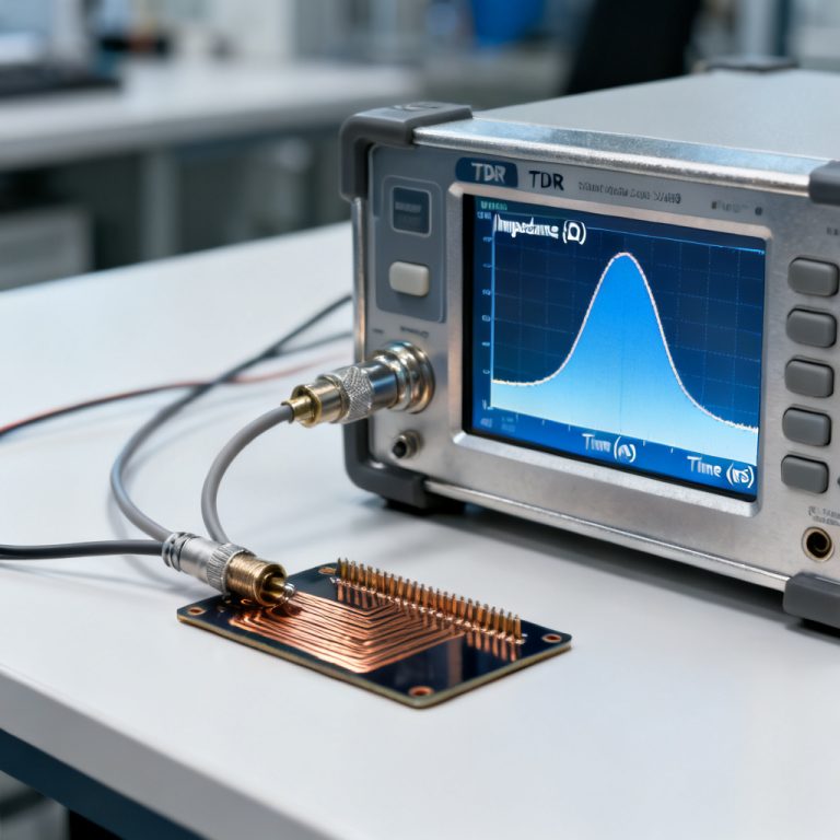
6.3 Validating with Measurements
Use a TDR to measure crosstalk on prototypes and compare with HyperLynx simulations to refine models.
7. Conclusion: Integrating HyperLynx into Your High-Speed PCB Workflow
Crosstalk simulation in high speed PCB using HyperLynx requires understanding electromagnetic coupling, careful pre-layout exploration, and rigorous post-layout validation. Always simulate with actual IBIS models, use the Crosstalk Wizard, run both time-domain and frequency-domain simulations, and document settings. This reduces prototype spins and improves first-pass success.
Frequently Asked Questions
What is crosstalk simulation in high speed PCB?
Crosstalk simulation in high speed PCB is the process of analyzing electromagnetic coupling between adjacent traces to predict and mitigate signal integrity issues using tools like HyperLynx.
Why is crosstalk simulation in high speed PCB important?
Crosstalk simulation in high speed PCB prevents false triggering, timing violations, and system failures by identifying coupling before fabrication.
How do I set up crosstalk simulation in high speed PCB using HyperLynx?
Set up crosstalk simulation in high speed PCB by defining stackup, creating coupled traces, assigning drivers, and running simulations in LineSim (pre-layout) or BoardSim (post-layout).
What are common crosstalk reduction techniques?
Common techniques include increasing trace spacing, adding guard traces, using differential signaling, and optimizing stackup design.
Can HyperLynx simulate differential pair crosstalk?
Yes, HyperLynx can simulate differential pair crosstalk as common-mode noise, requiring tight intra-pair coupling and adequate inter-pair spacing.