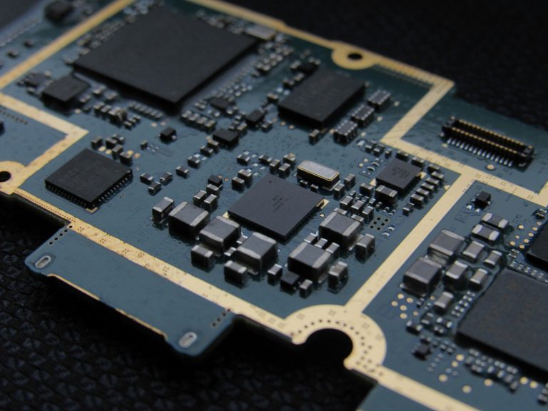
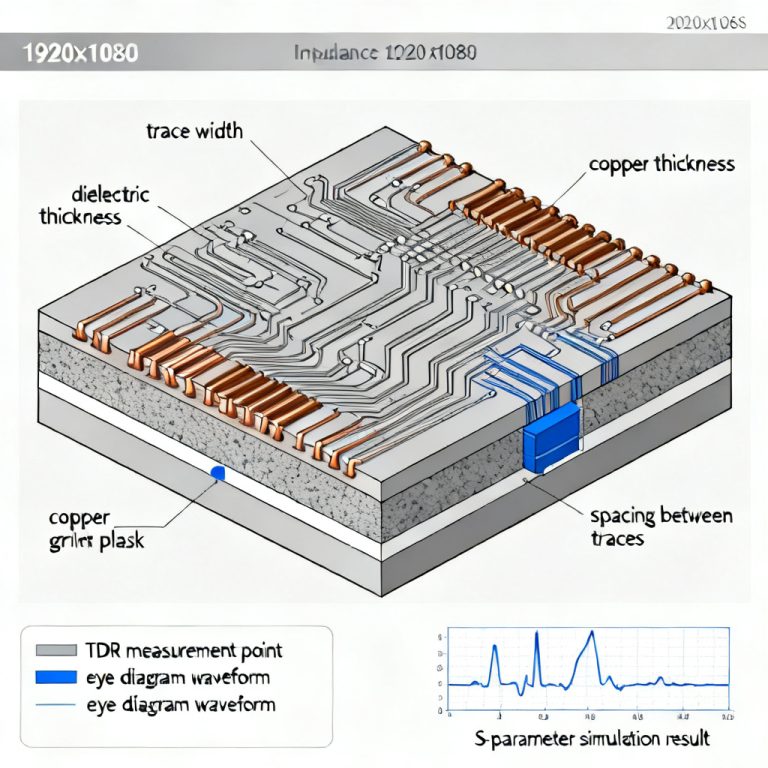
High-speed PCB design relies heavily on differential pair routing rules to maintain signal integrity, suppress common-mode noise, minimize crosstalk, and reduce EMI radiation. With the rapid upgrade of high-speed interfaces such as PCIe 5.0, USB 4, and 100G-KR4, improper differential layout easily causes impedance discontinuity, signal skew, bit errors, and system instability. Mastering differential pair routing rules is essential for every PCB designer.
This ultimate pillar guide integrates industry authoritative standards from Cadence, Texas Instruments, and Altium, covering basic principles, three core routing rules, length matching & phase tuning, gap coupling control, corner geometry design, via & reference plane constraints, crosstalk isolation, protocol-specific parameters, design checklist, common mistakes, and practical FAQs. As covered in our PCB Design Guidelines, proper differential pair routing rules directly impact signal integrity and system reliability.
Table of Contents
- 1. What Are Differential Pair Routing Rules & Why They Matter
- 2. Three Core Fundamental Rules of Differential Pair Routing
- 3. Differential Pair Length Matching & Phase Tuning Standards
- 4. Gap Control, S/W Ratio & Coupling Strength Classification
- 5. Corner Geometry & Forbidden Routing Shapes for Diff Pairs
- 6. Via Placement, Return Path & Reference Plane Design Rules
- 7. Crosstalk Isolation Rules Between Adjacent Differential Pairs
- 8. High-Speed Protocol Specific Differential Pair Requirements
- 9. Complete Differential Pair Routing Design Checklist
- 10. Common Mistakes to Avoid in High-Speed Differential Layout
- 11. Key Takeaways
- 12. FAQ About Differential Pair Routing Rules
- 13. Professional PCB Design Support & Custom Layout Inquiry
What Are Differential Pair Routing Rules & Why They Matter
A differential pair refers to two parallel transmission lines routed together, working with equal trace length, fixed spacing, and opposite-phase signal transmission. Differential pair routing rules are a set of standardized layout constraints formulated for high-speed PCB design, controlling trace length, gap, coupling, corner shape, via placement, reference plane, and isolation distance. Understanding these differential pair routing rules is the first step toward reliable high-speed design.
The core purposes of following standard differential pair routing rules are:
- Maintain stable controlled differential impedance along the entire signal path
- Suppress common-mode noise and improve anti-interference ability
- Effectively reduce EMI radiation and electromagnetic compatibility risks
- Eliminate signal skew, reflection, and bit error issues in high-speed transmission
- Comply with official specifications of PCIe, USB, Ethernet, and other high-speed protocols
At high data rates above gigabits per second, casual routing without rule constraints will lead to impedance mutation, unbalanced phase, severe crosstalk, and unstable link training. For industrial equipment, server motherboards, consumer high-speed terminals, and communication base station PCBs, strictly implementing differential pair routing rules is the foundation of reliable mass production.
Three Core Fundamental Rules of Differential Pair Routing
All high-speed differential pair layout is built on three non-negotiable core rules; any violation will directly damage signal integrity performance.
Length Matching
Keep the length deviation within 2–5 mil for general high-speed differential pairs. Mismatched trace lengths generate timing skew, break phase balance of complementary signals, increase common-mode noise, and weaken noise rejection capability. Advanced protocols such as USB 4 and PCIe 5.0 require even tighter length tolerance.
Constant Gap
The spacing (S) between the two traces of a differential pair must remain completely unchanged throughout straight lines, corners, fanout, and layer transition. Sudden expansion or narrowing of the gap causes impedance discontinuity and signal reflection.
Tight Coupling
Follow the standard S ≤ 2W (S = differential gap, W = single trace width). Tight coupling enhances magnetic field cancellation between two traces, stabilizes differential impedance, and optimizes EMI suppression. Loose coupling beyond 2W will make differential pairs behave like two independent single-ended lines, losing the inherent advantages of differential signaling.
These three rules run through the whole layout process, and their impact on characteristic impedance is explained in our Impedance Matching Ultimate Guide, which covers the Zdiff formula and tolerance guidelines. Following these differential pair routing rules ensures consistent impedance throughout the signal path.
Differential Pair Length Matching & Phase Tuning Standards
Length matching is the most critical tuning step for high-speed differential pairs, and different interfaces have clear mil-level tolerance requirements.
Protocol Length Tolerance Standard
- PCIe 5.0: Intra-pair length mismatch controlled within 2–3 mil
- USB 4: Strictest requirement, controlled within 1–2 mil
- 100G-KR4: Intra-pair deviation limited to 2–3 mil
Serpentine Routing Design Rules
When natural routing cannot meet equal-length requirements, serpentine routing is used for phase compensation, and must follow geometric limits to avoid additional interference:
- Serpentine bulge height ≤ 3 × W
- Spacing between adjacent serpentine segments ≥ 4 × W
- Avoid dense and irregular folding to prevent extra crosstalk and impedance fluctuation
Multi-Lane Alignment Requirement
For multi-channel interfaces like multi-lane PCIe and 100G Ethernet, not only intra-pair length matching is required, all differential lanes need length alignment at the receiver end. Synchronous signal arrival ensures stable sampling, reduces inter-lane skew, and lowers system bit error rate.
Gap Control, S/W Ratio & Coupling Strength Classification
The S/W ratio determines coupling degree, impedance stability, and noise suppression effect. Engineers must select reasonable coupling strength according to application scenarios.
| S/W Ratio | Coupling Level | Application Recommendation |
|---|---|---|
| ≤ 1W | Strong Coupling | Preferred for PCIe 5.0, USB4, 100G high-speed design |
| 1W ~ 2W | Medium Coupling | Suitable for general high-speed interfaces |
| > 2W | Weak Coupling | Not recommended for high-speed PCB |
High-speed PCB design should default to S ≤ 2W tight coupling. Do not arbitrarily widen the differential gap for layout convenience; if space is limited, adjust trace width proportionally to keep the S/W ratio unchanged, rather than breaking the constant gap rule. This is a key aspect of differential pair routing rules that many designers overlook.
Corner Geometry & Forbidden Routing Shapes for Diff Pairs
Corner structure directly affects impedance continuity and length matching accuracy; different bending methods have clear allowable and forbidden standards.
✅ Recommended Routing Corners
- Arc corner: The optimal solution for high-speed differential pairs. Smooth transition without geometric mutation, maintains continuous impedance and minimizes signal reflection.
- 45° / 135° oblique corner: Excellent manufacturability and signal performance, widely used in commercial and industrial high-speed PCB projects.
❌ Strictly Forbidden
- Right-angle corner: Causes local equivalent trace width mutation, impedance spike, signal reflection, and increased EMI radiation, completely prohibited for high-speed differential pairs.
Key Layout Note
When bending differential pairs, keep two traces synchronous bending at all times. Asymmetric corners will produce natural length deviation; designers need to make synchronous compensation for inner and outer corners to guarantee equal length after turning. Avoid staggered bending and offset path layout.
Via Placement, Return Path & Reference Plane Design Rules
Via transition and reference plane integrity are the most vulnerable points of differential pair signal integrity; non-standard via design easily causes phase imbalance and return path interruption. The return path principles discussed in our Return Path Design Guide — specifically how reference plane continuity affects differential signals — apply directly to differential pair routing as part of differential pair routing rules.
Symmetric Via Layout
The two vias of one differential pair must adopt the same aperture, pad size, and symmetrical position, ensuring consistent transmission delay and phase synchronization. Asymmetric vias introduce extra skew and destroy length matching effects. For complete via design parameters including back drilling and stub control, see our High-Speed PCB Via Design Guide.
Return Ground Via Configuration
Place 1–2 adjacent ground vias next to each differential signal via. Ground vias provide low-impedance return current paths, suppress via stub resonance, reduce crosstalk, and restrain EMI radiation.
Reference Plane No Split Rule
Differential pairs are strictly forbidden to cross reference plane splits. Complete and uninterrupted ground or power reference planes must be kept under the routing path. Crossing split slots cuts off the return current path, triggers severe impedance fluctuation, and leads to obvious signal integrity degradation. Priority should be given to inner-layer routing with complete reference planes; when layer transition is unavoidable, minimize via stub length and keep fanout traces short and symmetric.
Crosstalk Isolation Rules Between Adjacent Differential Pairs
In dense multi-lane high-speed PCB layout, inter-pair crosstalk is a main cause of communication interference and intermittent failure. The physics of capacitive and inductive coupling — explained in our Crosstalk Guide — shows that proper spacing is essential for differential pair isolation and must be included in your differential pair routing rules.
- Pair-to-pair spacing standard: ≥ 4W or fixed distance ≥ 20mil, take the stricter one as the design standard
- Avoid long-distance parallel routing of multiple differential pairs on the same layer; long parallel sections accumulate coupling interference
- Multi-layer PCB adopts vertical cross layout for differential pairs on different layers, avoiding overlapping parallel routing
- Keep high-speed differential pairs away from clock traces, switching power lines, and high-frequency noise circuits without insufficient isolation
Following the above rules can effectively suppress near-end and far-end crosstalk, maintain signal margin, and ensure stable operation of multi-channel high-speed interfaces.
High-Speed Protocol Specific Differential Pair Requirements
Different high-speed serial protocols have customized standards for differential impedance, intra-pair length matching, and pair-to-pair spacing, which cannot be unified with general rules. Applying these protocol-specific differential pair routing rules ensures compatibility and certification.
| Protocol | Differential Impedance | Intra-Pair Length Mismatch | Pair-to-Pair Isolation |
|---|---|---|---|
| PCIe 5.0 | 100Ω | 2–3 mil | ≥ 4W |
| USB 4 | 90Ω | 1–2 mil | ≥ 4W |
| 100G-KR4 | 100Ω | 2–3 mil | ≥ 20mil |
PCIe 5.0 and 100G-KR4 adopt classic 100Ω differential impedance, suitable for server and data center high-rate transmission. USB 4 uses 90Ω impedance with ultra-strict 1–2 mil length tolerance to adapt to complex interference scenarios of consumer and mobile devices. Designers should lock protocol parameters in PCB constraint rules in the early stage of design to avoid manual modification errors and mass production compatibility risks.
Complete Differential Pair Routing Design Checklist
Before completing PCB layout and DRC inspection, use this checklist for one-click self-verification to eliminate hidden risks. Following this checklist ensures all differential pair routing rules are properly implemented:
- Intra-pair length matching fully meets the corresponding protocol mil-level tolerance
- Differential gap keeps constant in the whole route without local shrinkage or widening
- Differential vias are arranged symmetrically in pairs, with matched adjacent ground return vias
- Try best to route on the same layer, strictly avoid crossing reference plane splits
- Pair-to-pair spacing meets ≥4W or 20mil standard, no long parallel overlapping
- No right-angle corners are used; arc or 45° corners are adopted uniformly
- Serpentine length tuning follows 3×W height and 4×W spacing limits
- Tight coupling S ≤ 2W is maintained for all high-speed differential pairs
Common Mistakes to Avoid in High-Speed Differential Layout
| Mistake | Consequence | Correct Practice |
|---|---|---|
| Random length tuning with irregular serpentine folding | Extra skew and crosstalk | Follow 3W/4W serpentine rules |
| Unilateral widening of differential gap | Impedance discontinuity | Keep constant gap throughout |
| Asymmetric via placement without ground return vias | Phase imbalance, poor return path | Symmetric vias + adjacent ground vias |
| Crossing reference plane splits | Return path broken, severe EMI | Keep continuous reference plane |
| Excessively loose coupling S > 2W | Loss of noise suppression | Maintain S ≤ 2W tight coupling |
Avoiding these common mistakes can greatly improve the yield and stability of high-speed PCB products. For a broader perspective on routing rules that apply to both single-ended and differential signals, see our High-Speed PCB Routing Rules guide.
Key Takeaways
- The core of differential pair routing rules lies in equal length, equal spacing, tight coupling — three principles must be implemented simultaneously
- Control general intra-pair length mismatch within 2–5 mil; high-end protocols like USB4 and PCIe 5.0 need stricter 1–3 mil tolerance
- Keep S ≤ 2W for tight coupling; S/W ratio directly determines coupling strength and signal performance
- Adopt arc or 45° corners only; prohibit right-angle bends, and ensure synchronous corner compensation
- Vias must be symmetric with matched ground return vias; never allow differential pairs to cross reference plane splits
- Pair-to-pair isolation ≥4W or 20mil; use vertical cross layout for multi-layer routing to reduce crosstalk
- Follow protocol-specific impedance, length and spacing parameters; complete checklist inspection before final design
FAQ About Differential Pair Routing Rules
Q1: What is the standard length mismatch for ordinary high-speed differential pairs?
General requirement is within 2–5 mil; PCIe 5.0 is 2–3 mil, USB4 needs 1–2 mil. This is a fundamental differential pair routing rules parameter.
Q2: Can differential pair gap be changed halfway?
No. Any gap change will cause impedance discontinuity and signal reflection; the whole section must keep constant spacing.
Q3: Why is right-angle corner forbidden for differential pairs?
Right angle leads to local impedance mutation, signal reflection, and increased EMI radiation, which seriously damages high-speed signal integrity.
Q4: How much spacing should be kept between two adjacent differential pairs?
Follow ≥4W or ≥20mil, take the larger one as the standard, and avoid long parallel routing.
Q5: Is it necessary to add ground vias beside differential signal vias?
Yes. 1–2 adjacent ground vias provide low-impedance return path, suppress resonance and reduce crosstalk.
Q6: What is the best S/W ratio for high-speed differential pairs?
S ≤ 2W is recommended; ≤1W is strong coupling with optimal performance, 1W–2W is medium coupling for general scenarios.
Get Professional Differential Pair Layout Review & Quote
Mastering all differential pair routing rules is the premise of high-speed PCB design, but actual project implementation involves stackup design, impedance calculation, protocol constraint setting, SI simulation, and DRC mass production verification, which requires rich engineering experience.
We offer: Free design scheme evaluation • Technical parameter consultation • High-speed PCB layout • Differential pair rule customization • Impedance stackup design • Design review • One-stop PCB manufacturing
Leave your project parameters and requirements now. We will reply with professional technical suggestions and a detailed quotation as soon as possible.
About
We are a specialized PCB design and manufacturing service provider serving industrial, automotive, medical, and communications OEMs worldwide. Our expertise in differential pair routing rules ensures your high-speed interfaces perform reliably. Return to the PCB Design Guidelines for more coverage of stackup design, routing rules, and DFM best practices.
© 2026 HighSpeedPCBs.com — Professional High-Speed PCB Solutions