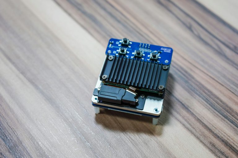
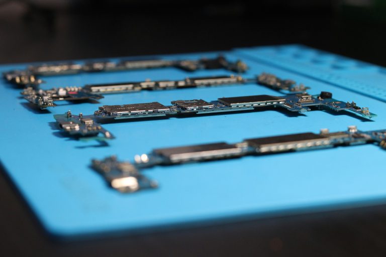
High-speed PCBs power modern CPUs, GPUs, FPGAs, SerDes interfaces, AI servers, and automotive electronic systems. As data rates exceed 25Gbps per channel and chip power density rises sharply, thermal accumulation becomes one of the biggest threats to system stability, signal integrity, component lifespan, and long-term reliability. Understanding thermal management high speed PCB is essential for every hardware engineer.
This ultimate pillar content covers fundamental thermal principles, heat source analysis, copper thickness optimization, thermal via array design, copper plane heat spreading, high thermal conductivity PCB materials, passive & active cooling, thermal and signal integrity trade-offs, design checklist, professional FAQs, and actionable engineering best practices. As covered in our PCB Design Guidelines, mastering thermal management high speed PCB is essential for reliable high-performance electronics.
Table of Contents
- 1. Introduction: Why Thermal Management Is Critical for High-Speed PCB
- 2. Heat Sources in Modern High-Speed PCB Systems
- 3. Copper Thickness Selection for Efficient Heat Spreading
- 4. Thermal Via Design Rules, Parameters and Layout Best Practices
- 5. Copper Pour & Solid Plane Layers for Heat Dissipation
- 6. PCB Substrate Materials: Thermal Conductivity Comparison & Selection
- 7. Heat Sinks, TIM Materials and Active Cooling Solutions
- 8. Thermal Design vs Signal Integrity: Key Trade-Offs & Solutions
- 9. Professional High-Speed PCB Thermal Management Checklist
- 10. Real Industry Applications: AI Server, Automotive & 5G RF PCB
- 11. Key Takeaways
- 12. FAQ About High-Speed PCB Thermal Management
- 13. Get Professional Thermal Design Review & Quotation
Introduction: Why Thermal Management Is Critical for High-Speed PCB
High-speed printed circuit boards are the core carrier of today’s high-performance electronic devices, including server CPUs, graphics GPUs, field-programmable FPGAs, ASIC chips, and 25Gbps+ SerDes high-speed differential interfaces. Compared with conventional low-speed PCBs, high-speed designs face dual strict constraints: stable signal integrity and effective thermal control. This is why thermal management high speed PCB must be prioritized from the start.
With the continuous improvement of chip integration and operating frequency, power consumption per unit area increases dramatically. Uncontrolled heat inside the PCB will trigger a chain of negative consequences:
- Automatic frequency reduction and system performance degradation
- Accelerated aging of PCB substrate, solder joints and component packaging
- Local hotspot formation leading to dielectric breakdown
- Shortened product service life and unexpected field failure
Thermal management high speed PCB is no longer an optional optimization step but a mandatory design discipline for mass production and long-term reliable operation. The entire thermal solution relies on three core passive foundations: copper foil heat spreading, thermal via vertical conduction, and solid copper plane heat dissipation, supplemented by heat sinks, thermal interface materials and forced air active cooling for high-power scenarios.
Well-executed thermal design also must coordinate with signal integrity, impedance control and EMI suppression. Ignoring either side will result in either overheating failure or high-speed signal distortion, crosstalk and transmission errors.
Heat Sources in Modern High-Speed PCB Systems
To optimize thermal design accurately, designers must first clarify all heat generation sources on high-speed PCBs. Each source overlaps and couples with each other, forming concentrated hotspots without reasonable layout isolation. Effective thermal management high speed PCB starts with identifying these sources.
High-Speed Core Chip Power Dissipation
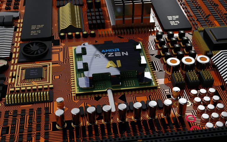
CPUs, GPUs, FPGAs and ASICs are the primary heat sources. These highly integrated ICs consume large power under full load, converting most electrical energy into heat that transfers downwards to the PCB substrate. Server-grade and AI accelerator chips especially feature ultra-high power density, putting extreme pressure on board-level thermal dissipation.
Power Conversion Losses
DC-DC switching regulators and LDO linear regulators inevitably produce energy loss during voltage conversion. The wasted power is completely converted into heat. Dense arrangement of power modules on high-speed PCBs easily creates continuous high-temperature zones.
High-Speed SerDes Interface Heat
Modern SerDes interfaces run at 25Gbps, 56Gbps or even higher per lane. Each high-speed channel consumes hundreds of milliwatts of power. Multi-channel parallel layout accumulates massive heat and forms concentrated thermal hotspots near routing areas. For routing rules that help manage this heat, see our High-Speed PCB Routing Rules guide, which complements thermal management high speed PCB strategies.
Resistive Copper Loss on High-Current Traces
High-current power paths and thick power traces generate Joule heat due to copper resistance. The larger the current and the longer the trace, the more obvious the thermal accumulation, which further raises the overall board temperature and affects adjacent high-speed sensitive circuits.
Copper Thickness Selection for Efficient Heat Spreading
Copper foil is the most cost-effective thermal spreading medium in PCB design. Higher copper thickness provides larger cross-sectional area, lower thermal resistance and stronger lateral heat diffusion capability, dispersing concentrated hotspot heat to a wider board area. Copper thickness selection is a fundamental decision in thermal management high speed PCB.
Standard Copper Weight & Thickness Specification
| Copper Weight | Copper Thickness | Typical Application Scenarios |
|---|---|---|
| 1 oz | 35 μm | General low-power signal layers, standard high-speed signal routing |
| 2 oz | 70 μm | High-current power traces, medium-power high-speed PCB thermal enhancement |
| 3 oz+ | 105 μm + | High-power CPU/GPU/FPGA zones, AI server, automotive high-power PCB |
Core Design Rules
- Arrange large-area complete copper pours directly below high-power chips on inner layers and bottom layers
- Avoid fragmented, segmented copper shapes that block lateral heat conduction paths
- Thickened copper not only improves heat spreading but also reduces high-current resistive loss and secondary heat generation
Design Constraint Reminder
Increased copper thickness will lower characteristic impedance of high-speed traces. The impedance principles discussed in our Impedance Matching Ultimate Guide must be applied here — designers must fine-tune trace width to maintain standard 50Ω single-ended or 100Ω differential impedance, making thermal management high speed PCB a balancing act.
Thermal Via Design Rules, Parameters and Layout Best Practices
Thermal vias are the key vertical thermal conduction structure of multi-layer high-speed PCBs. They transfer heat from top-layer component pads vertically down to inner ground planes and bottom copper pours, building a 3D heat dissipation channel. Without proper thermal via arrays, heat will be trapped on the top layer and cannot diffuse downward. For detailed via design principles including back drilling, see our High-Speed PCB Via Design Guide, which is essential for thermal management high speed PCB.
Recommended Thermal Via Standard Parameters
| Parameter | Recommended Value | Engineering Purpose |
|---|---|---|
| Via Hole Diameter | 0.2 – 0.3 mm | Balance conduction area and manufacturing safety margin |
| Array Pitch | 1.0 – 1.2 mm | Dense enough for low thermal resistance without occupying routing space |
| Filling Method | Solid Copper Filled | Eliminate internal air gaps, maximize thermal & electrical conductivity |
| Layout Pattern | Grid / Staggered | Uniform heat distribution, no thermal dead zones |
Practical Layout Experience
- High-power BGA, QFN and power devices should deploy at least 4×4 thermal via array under the central pad area
- Grid layout suits regular chip outlines; staggered layout performs better for irregular high-power component placement
- Fully copper-filled thermal vias outperform ordinary plated vias significantly in long-term high-temperature operation
DFM & SI Avoidance Tips
Do not arrange dense thermal via arrays close to high-speed differential pairs, to prevent crosstalk and capacitive coupling interference. Adopt back-drilling technology to eliminate via stubs and reduce high-frequency signal attenuation.
Copper Pour & Solid Plane Layers for Heat Dissipation
Thermal vias provide vertical conduction, while complete copper pours and solid plane layers undertake lateral heat spreading. The two must cooperate to form an integrated heat dissipation network. This combination is a cornerstone of effective thermal management high speed PCB.
Plane Layer Layout Strategy
- Lay intact solid ground or power planes on inner layers directly beneath CPUs, GPUs and FPGAs
- Avoid arbitrarily splitting complete planes with routing; broken planes will seriously block heat spreading and damage high-speed signal return paths
- Connect multiple ground layers through dense thermal vias to realize synchronous heat diffusion across all layers
Heat Dissipation Copper Area Rule
The coverage area of thermal copper pour should be 2 to 3 times the projection area of the high-power component. The oversized layout provides sufficient margin for lateral heat diffusion and prevents heat from being limited to a small local zone.
Multi-Chip Thermal Isolation
For high-speed PCBs with multiple high-power chips, configure independent large-area copper regions for each device and reserve isolation gaps between thermal zones to avoid mutual thermal coupling and temperature superposition.
PCB Substrate Materials: Thermal Conductivity Comparison & Selection
PCB substrate material determines the inherent natural heat conduction capability of the entire board. Material selection at the stackup stage directly affects the difficulty of subsequent copper layout and thermal via design. The stackup principles covered in our Stackup Design Guide must account for thermal conductivity requirements as part of thermal management high speed PCB.
Common PCB Material Thermal Conductivity & Application
| PCB Material | Thermal Conductivity (W/m·K) | Application Scenarios |
|---|---|---|
| Standard FR4 | 0.3 – 0.4 | Low-speed, low-power consumer electronics |
| High Tg FR4 | 0.4 – 0.5 | General high-speed digital PCB, industrial control high-speed board |
| Metal Core PCB | 1 – 3 | High-power LED, automotive electronics, high-current modules |
| Ceramic Filled Substrate | 2 – 4 | 5G RF high-frequency board, base station high-power PCB |
Selection Guidelines
- Standard FR4 is cost-effective but low in thermal conductivity, only suitable for low-power low-speed designs
- High Tg FR4 is the mainstream choice for most commercial high-speed PCBs, with better temperature resistance and moderate thermal performance
- Metal core substrates are preferred for scenarios requiring rapid heat dissipation and high mechanical stability
- Ceramic filled materials feature low dielectric loss and high thermal conductivity, ideal for high-frequency RF and 5G high-speed applications
Heat Sinks, TIM Materials and Active Cooling Solutions
For ultra-high-power high-speed boards such as AI server and high-end computing hardware, passive thermal design with copper and thermal vias alone cannot control hotspot temperature. It is necessary to match heat sinks, thermal interface materials and active cooling methods. These advanced solutions complement basic thermal management high speed PCB techniques.
Heat Sink & Thermal Interface Material (TIM)
- Mount customized aluminum or copper heat sinks on high-power chip surfaces
- Fill gaps between chip shell and heat sink with thermal pads, thermal grease or thermal adhesive to eliminate air isolation
Forced Air Cooling
In enclosed equipment with poor natural convection, adopt fan forced air cooling to accelerate air flow on PCB surface, take away heat from heat sinks and copper planes
High-Speed Design Special Attention
Metal heat sinks may break high-speed signal ground return paths and introduce capacitive coupling interference. Designers must maintain ground plane integrity under high-speed routing, perform reliable grounding and shielding for metal heat sinks, and avoid placing heat sink mounting structures across differential pair routing channels.
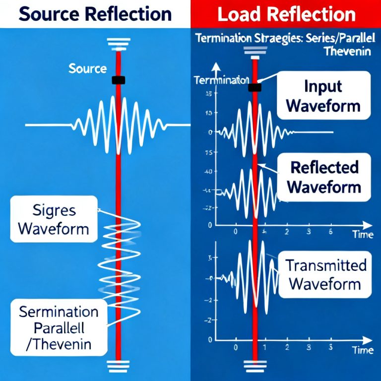
Thermal Design vs Signal Integrity: Key Trade-Offs & Solutions
Thermal optimization and signal integrity (SI) are often mutually restricted in high-speed PCB design. Blindly enhancing heat dissipation will damage signal quality; overemphasizing SI will cause insufficient thermal margin. Designers need to master balanced optimization strategies. This is one of the most challenging aspects of thermal management high speed PCB.
| Thermal Measure | Impact on Signal Integrity | Optimized Solution |
|---|---|---|
| Increase copper thickness | Reduce characteristic impedance | Narrow trace width appropriately to compensate impedance deviation |
| Dense thermal vias | Generate via stubs & crosstalk | Use back-drilling to remove redundant stubs; keep away from differential pairs |
| Mount metal heat sinks | Capacitive coupling interference | Solid grounding + shielding isolation near sensitive high-speed lines |
High-temperature environment will also raise substrate dielectric constant, change impedance parameters, and increase crosstalk and signal attenuation. Thermal simulation and SI simulation should be carried out simultaneously in the early layout stage to achieve coordinated optimization.
Professional High-Speed PCB Thermal Management Checklist
Use this checklist during stackup design, layout review, and DFM inspection to avoid thermal design omissions and post-production overheating risks. Following these thermal management high speed PCB guidelines ensures first-pass success:
- Arrange minimum 4×4 thermal via array under all high-power CPU, GPU, FPGA and power semiconductor components
- Deploy large-area intact copper pours on inner and bottom layers, covering 2–3 times component projection area
- Adopt 2oz or heavier copper foil for high-current paths and key thermal zones to reduce resistive heat loss
- Reserve unobstructed air convection channels on PCB and chassis layout; do not cluster high-power devices in narrow confined spaces
- Select high Tg or high thermal conductivity substrate for high power density high-speed PCB
- Run thermal simulation under full load to identify hotspots and optimize layout before manufacturing
- Keep thermal vias and thick copper areas away from high-speed differential pairs to avoid SI interference
- Match suitable heat sinks and TIM materials for high-power chips; ensure ground continuity after heat sink installation
Real Industry Applications: AI Server, Automotive & 5G RF PCB
AI Server High-Speed PCB
AI accelerators and server GPUs feature ultra-high power consumption and dense SerDes channels. Design relies on 3oz thick copper, dense thermal via arrays, multi-layer complete ground planes, plus heat sink + forced air cooling to control junction temperature. Effective thermal management high speed PCB is critical for AI server reliability.
Automotive High-Speed PCB
Automotive ADAS, vehicle Ethernet and intelligent cockpit PCBs face high ambient temperature and high reliability requirements. Adopt high Tg FR4 or metal core substrate, optimized thermal via layout, and strictly balance thermal design with EMC & signal integrity.
5G RF High-Frequency PCB
5G base station and RF high-speed boards use ceramic filled high thermal conductivity materials. Thermal design must coordinate with low dielectric loss requirements, avoid thermal structures interfering with RF impedance and radiation performance.
Key Takeaways
- Thermal management high speed PCB relies on the trinity of reasonable copper thickness, standardized thermal via arrays, and complete copper plane heat spreading
- Control thermal via array pitch within 1.0–1.2mm and adopt solid copper filling to ensure vertical heat conduction efficiency
- PCB material selection must match power density, operating frequency and cost budget to balance thermal conductivity and dielectric performance
- High-power scenarios need to add heat sinks, thermal interface materials and active forced air cooling as supplementary solutions
- Thermal design and signal integrity must be optimized synchronously; every thermal structure adjustment needs to consider impedance, return path and crosstalk suppression
- Follow the standard thermal checklist and thermal simulation verification to avoid mass production failures and field reliability risks
FAQ About High-Speed PCB Thermal Management
Q1: What is the most cost-effective thermal solution for high-speed PCB?
Using 2oz copper foil + standard 4×4 thermal via array + large-area bottom copper pour is the most cost-effective passive solution, suitable for most medium-power high-speed boards without extra heat sinks. This is a core principle of thermal management high speed PCB.
Q2: Why cannot thermal vias be arranged too close to high-speed differential pairs?
Dense vias cause capacitive coupling, destroy differential impedance balance, induce crosstalk and signal phase deviation, deteriorating high-speed signal integrity.
Q3: Is 1oz copper enough for high-speed PCB thermal design?
1oz (35μm) is only suitable for low-power signal layers. High-current and high-power chip thermal zones must use 2oz or above thickened copper for effective thermal management high speed PCB.
Q4: What is the best thermal via filling method?
Solid copper filled vias are the best choice, eliminating internal air gaps and providing the highest thermal and electrical conductivity for long-term high-temperature operation.
Q5: How to balance thermal design and signal integrity?
Optimize layout in advance, keep thermal structures away from sensitive high-speed lines, compensate impedance for thick copper, use back-drilling for via stubs, and perform thermal & SI co-simulation.
Get Professional Thermal Design Review & Custom Solution
Do you have ongoing high-speed PCB projects for AI server, automotive electronics, 5G RF or industrial high-speed systems? Are you troubled by hotspot overheating, unreasonable thermal via layout, copper thickness selection confusion, or conflicts between heat dissipation and signal integrity routing? Our team specializes in thermal management high speed PCB for complex high-power designs.
We offer: Free thermal layout review • Stackup suggestion • Thermal via parameter optimization • Heat dissipation scheme evaluation • Custom PCB manufacturing quotation
Send your project details now. We will reply with professional technical feedback and personalized quotation as soon as possible.
About HighSpeedPCBs.com
We are a specialized PCB design and manufacturing service provider serving industrial, automotive, medical, and communications OEMs worldwide. Our expertise in thermal management high speed PCB ensures your high-speed designs are thermally stable and electrically reliable. Return to the PCB Design Guidelines for more coverage of stackup design, routing rules, and DFM best practices.
© 2026 HighSpeedPCBs.com — Professional High-Speed PCB Solutions