[rank_math_breadcrumb]
In high-speed digital and RF applications, a Differential Pair Impedance Coupon is essential for verifying that controlled impedance targets (e.g., 100Ω differential, 90Ω USB, 85Ω PCIe) are met during PCB fabrication. A single mismatch can cause signal reflection, crosstalk, and timing errors. This comprehensive guide synthesizes authoritative insights from top industry sources to provide a complete methodology for designing differential pair impedance test coupons.
Core Principles of Differential Pair Impedance Coupon Design
1.1 What Is an Impedance Coupon?
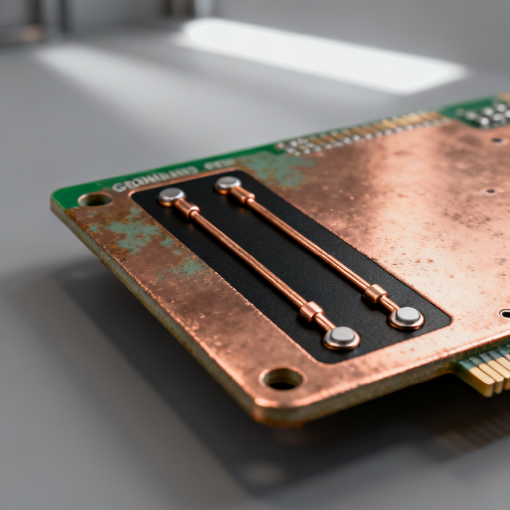
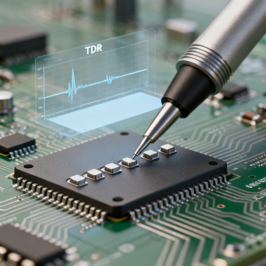
An impedance coupon is a short, dedicated trace (or pair of traces) that replicates the exact physical characteristics of the actual high-speed signal lines on your PCB. It is placed on the panel—usually near the edge or in a designated test area—so that a Time Domain Reflectometer (TDR) can measure the characteristic impedance without disturbing the functional circuit.
Key attributes:
- Must have the same copper weight, trace width, spacing, dielectric material, and layer stack-up as the target differential pair.
- Must be long enough to allow a clean TDR measurement (typically 3 to 6 inches or 75–150 mm).
- Must include clear reference planes (ground or power) identical to the actual design.
1.2 Why Differential Pairs Require Separate Coupons
Differential pairs are more sensitive to manufacturing variations than single-ended traces. Impedance depends not only on trace geometry but also on coupling (spacing) between the two lines. A differential coupon must preserve:
- Differential impedance (Zdiff): The impedance between the two lines.
- Odd-mode impedance (Zodd): The impedance of each line with respect to ground, when driven differentially.
- Common-mode impedance (Zcomm): The impedance of both lines driven together.
Coupon Placement and Panel Location
2.1 Standard Placement Rules
Coupons must be placed within the production panel—not on a separate test coupon panel—to reflect the actual manufacturing conditions. Place them:
- Along the panel edge (top, bottom, or side), at least 0.5 inches from the board outline to avoid edge effects.
- In the same orientation as the real traces (horizontal vs. vertical) to account for fiber weave and copper grain direction.
- On every layer where differential pairs are routed. Do not assume one coupon represents all layers.
2.2 Avoiding Proximity Effects
Avoid placing coupons too close to large copper pours, via arrays, or board edges. These create:
- Impedance deviations due to changed return current paths.
- Etching variations near copper boundaries.
Rule: Maintain a minimum 5x the trace width clearance from any other copper feature.
2.3 Multiple Coupons for Different Impedance Targets
Include separate coupons for each unique impedance target in your design. For example:
- 100Ω differential for USB/HDMI
- 90Ω differential for PCIe Gen4
- 85Ω differential for DDR5
Do not combine them into one long trace; use individual coupons labeled clearly.
Coupon Geometry and Dimensions
3.1 Trace Length
Minimum 3 inches (75 mm), with 4–6 inches preferred. Shorter traces cause TDR reflections from the launch point to interfere with the measurement. For very high-speed signals (>10 Gbps), use 6 inches to allow for a longer TDR window and to average out local impedance variations.
3.2 Trace Width and Spacing
- Width: Must match the target differential pair width exactly (e.g., 5 mils for 100Ω on a standard stack-up).
- Spacing (gap): Must match the edge-to-edge spacing of the differential pair. Do not use center-to-center spacing.
- Tolerance: Coupon traces should be designed with ±10% of target width to allow for manufacturing variation—but the actual measured impedance is the final validation.
3.3 Launch Pad and Probe Points
- Launch pad: A small, rectangular pad (e.g., 20 mil x 30 mil) at each end of the coupon, connected to the trace via a short taper.
- Ground pads: Two ground pads flanking the signal launch, spaced to match a standard TDR probe (e.g., 100 mil pitch for GSG probes).
- Via stubs: Avoid vias in the coupon path. If vias are unavoidable (e.g., for inner-layer coupons), use back-drilling or microvias to minimize stub resonance.
3.4 Multiple Coupon Types for Different Test Methods
- Single-ended coupons: For measuring Z0 of each line individually.
- Differential coupons: For measuring Zdiff directly.
- Hybrid coupons: A single differential pair with both ends accessible for both single-ended and differential TDR.
Recommendation: Include at least one differential coupon and one single-ended coupon for each layer and impedance target.
Stack-Up and Reference Plane Requirements
4.1 Exact Layer Replication
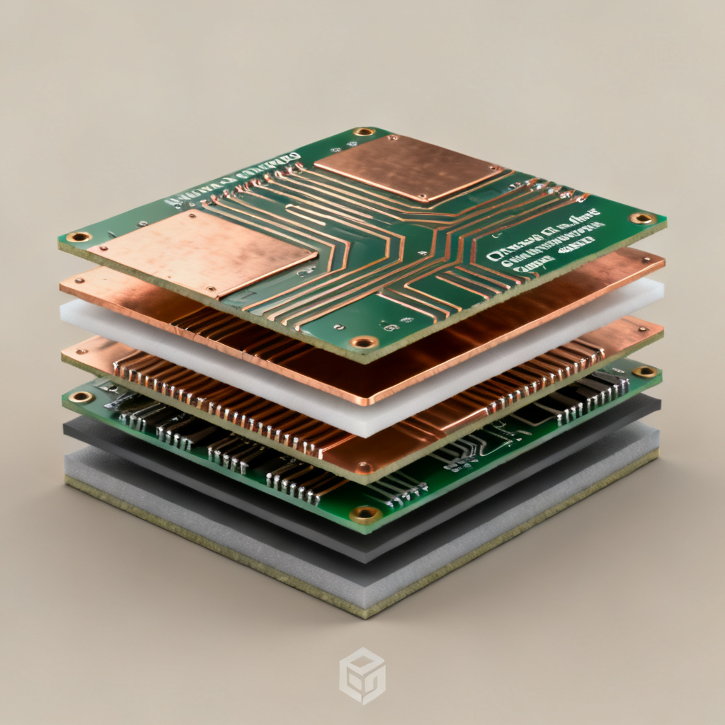
The coupon must be built on the same layer as the target differential pair, with identical reference planes above and below. For a microstrip differential pair on layer 1 (top), the coupon must also be on layer 1, with layer 2 as a solid ground plane. Do not use a different stack-up for the coupon. For a stripline differential pair (e.g., on layer 3 between two ground planes), the coupon must be on layer 3, with layers 2 and 4 as solid planes. No voids or splits.
4.2 Dielectric Thickness
Prepreg vs. core thickness variations are the largest source of impedance error. The coupon must use the same prepreg layup (e.g., 1080, 2116, 7628) as the actual board area. If the real traces run over a mix of prepreg and core, the coupon should represent the worst-case (usually the thinnest dielectric) or include multiple coupons for each dielectric zone.
4.3 Copper Weight and Etch Factor
- Copper weight: Must match (e.g., 1 oz, 0.5 oz).
- Etch factor: The trapezoidal cross-section of etched traces affects impedance. Coupons must be designed with the same target trace width at the bottom as the real traces. Use the manufacturer’s etch compensation in the coupon design.
Testing Methodology and Interpretation
5.1 TDR Setup
- Use a TDR with a rise time of 35–50 ps (or faster for >10 Gbps signals).
- Calibrate with a known impedance standard (e.g., 50Ω or 100Ω).
- Probe the coupon using a GSG (Ground-Signal-Ground) probe for single-ended or a GSGSG probe for differential.
5.2 Reading the Results
- Impedance profile: The TDR graph should show a flat region over the middle 60% of the trace length. Ignore the first 10% and last 10% (launch and termination effects).
- Acceptable tolerance: ±10% of target impedance (e.g., 90–110Ω for a 100Ω target). For high-speed designs, ±5% is preferred.
5.3 Common Failures and Solutions
| Failure | Cause | Solution |
|---|---|---|
| Impedance too low | Trace too wide or dielectric too thin | Narrow trace or increase dielectric thickness |
| Impedance too high | Trace too narrow or dielectric too thick | Widen trace or reduce dielectric thickness |
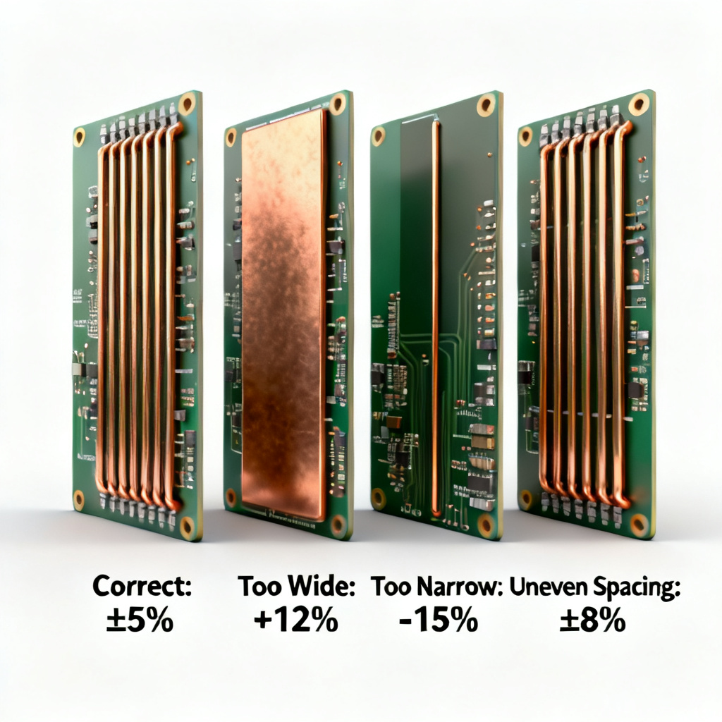
| Impedance varies along trace | Uneven etching or fiber weave effect | Adjust etch compensation or use spread-glass prepreg |
| Coupling mismatch | Uneven spacing between differential lines | Check artwork alignment and etching uniformity |
5.4 Correlation to Real Board Performance
The coupon is a predictor, not a perfect replica. Factors like adjacent traces, via stubs, and power plane splits on the real board can shift impedance. Use coupon measurements to:
- Validate the fabrication process.
- Fine-tune the stack-up for future runs.
- Provide a baseline for simulation-to-measurement correlation.
Advanced Considerations and Best Practices
6.1 Multiple Coupons per Panel
For large panels (e.g., 18” x 24”), place at least two coupons—one near the top and one near the bottom—to detect process variation across the panel.
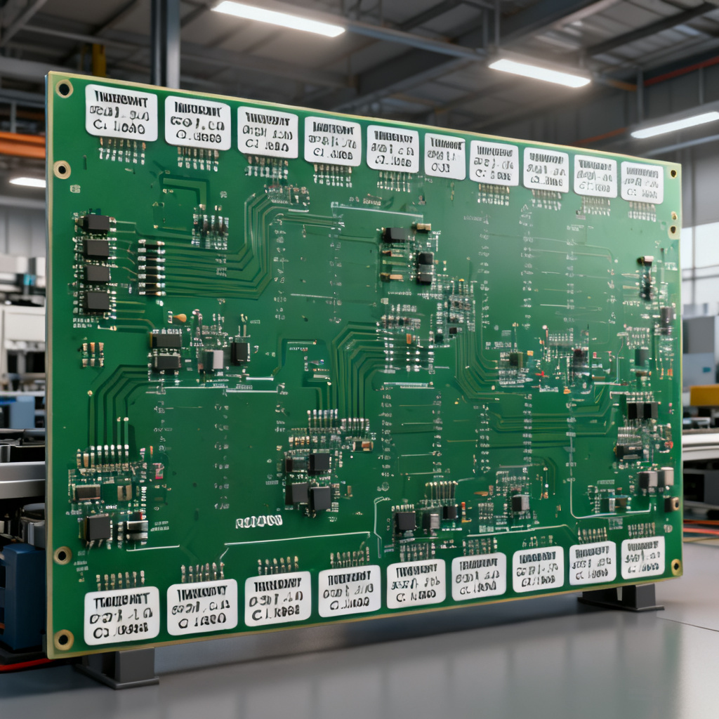
6.2 Labeling and Documentation
- Silkscreen labels: Include target impedance, layer number, and trace length (e.g., “100Ω DIFF L1 4in”).
- Fab notes: Specify that coupons must be measured with a TDR and reported in the impedance test report.
6.3 Avoiding Over-Design
Do not overcomplicate coupons with extra features like test points, vias, or bends. A straight, uniform trace is best. If bends are necessary (e.g., to fit the panel edge), use 45-degree mitered bends with a radius >3x trace width.
6.4 Simulation Before Fabrication
Before sending the design to manufacturing, run a 2D field solver (e.g., Polar Si9000, Ansys Q2D) to verify that the coupon geometry will yield the target impedance. Adjust width and spacing as needed.
Step-by-Step Design Checklist
- Identify all unique differential pair targets in your design (impedance, layer, reference planes).
- For each target, create a dedicated coupon trace:
- Length: 4–6 inches (100–150 mm).
- Width and spacing: Exact match to the real pair.
- Launch pads: GSG or GSGSG probe pads at both ends.
- Place coupons on the panel edge (top/bottom/side), min 0.5” from board outline.
- Ensure exact stack-up replication (same layer, same dielectric, same copper weight).
- Add clear silkscreen labels and fab notes.
- Simulate the coupon geometry with a field solver.
- Review with your PCB manufacturer for any fab-specific rules (e.g., minimum coupon size, panel utilization).
A well-designed Differential Pair Impedance Coupon is your first line of defense against signal integrity failures. By following the combined wisdom of top industry sources—covering placement, geometry, stack-up, and testing—you ensure that your high-speed PCB will perform as intended. The coupon is not optional. It is a required deliverable for any B2B high-speed PCB production. Use it to build trust with your customers and to guarantee that your manufacturing process delivers consistent, reliable impedance control.
Frequently Asked Questions
What is the minimum length for a differential pair impedance coupon?
The minimum recommended length for a Differential Pair Impedance Coupon is 3 inches (75 mm), with 4–6 inches preferred for high-speed signals above 10 Gbps to allow clean TDR measurements.
How many impedance coupons should I include on a panel?
You should include at least one Differential Pair Impedance Coupon per unique impedance target and per layer. For large panels, place two coupons (top and bottom) to detect process variation.
Can I use the same coupon for single-ended and differential measurements?
Yes, a hybrid coupon with accessible ends for both single-ended and differential TDR is recommended, but separate coupons for each test method are more reliable for accurate Differential Pair Impedance validation.
What causes impedance variation in a coupon?
Common causes include uneven etching, fiber weave effects, incorrect dielectric thickness, and proximity to copper features. Proper design and simulation mitigate these issues for a reliable Differential Pair Impedance Coupon.
How do I interpret TDR results from a differential coupon?
Focus on the middle 60% of the impedance profile, ignoring the first and last 10%. Acceptable tolerance is ±10% of target, with ±5% preferred for high-speed designs. This ensures your Differential Pair Impedance Coupon meets specification.