[rank_math_breadcrumb]
Differential pair impedance design in Altium Designer is critical for high-speed PCB signal integrity. This guide covers complete setup and validation workflows for USB, HDMI, PCIe, and LVDS interfaces.

Fundamentals of Differential Pair Impedance
What is Differential Impedance?
Differential pair impedance (Zdiff) is the impedance between the two traces of a differential pair when driven by a differential signal. It is typically twice the odd-mode impedance (Zodd) of each trace relative to the reference plane. For example, a 100Ω differential pair requires each trace to have an odd-mode impedance of 50Ω.
Key parameters influencing Zdiff include:
- Trace width (W) and spacing (S)
- Dielectric constant (Dk) and loss tangent (Df) of the substrate
- Copper thickness (T) and solder mask thickness
- Reference plane proximity (height H to the nearest ground plane)
Common Differential Impedance Targets
- USB 2.0/3.0: 90Ω differential (with 45Ω single-ended)
- HDMI: 100Ω differential (with 50Ω single-ended)
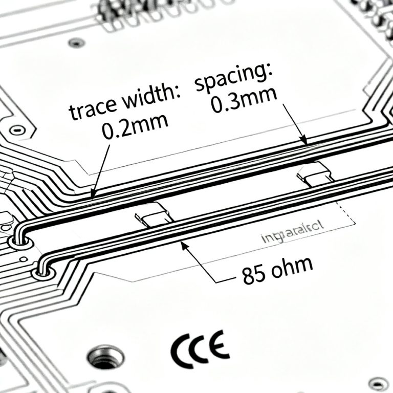
- PCIe Gen3/4: 85Ω differential (with 42.5Ω single-ended)
- Ethernet (1000BASE-T): 100Ω differential
- LVDS: 100Ω differential
The Role of Stackup
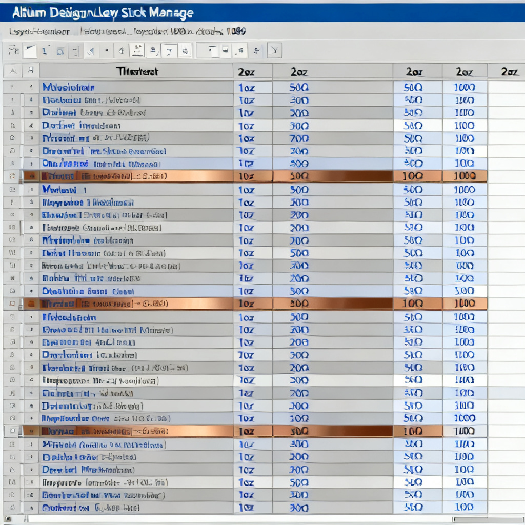
A controlled impedance stackup is non-negotiable. For differential pairs, use a symmetric stripline (inner layers) or microstrip (outer layers) configuration. Stripline offers better EMI shielding and lower crosstalk, while microstrip provides easier access for probing. Altium Designer’s Layer Stack Manager allows you to define dielectric materials, thicknesses, and copper weights.
Setting Up Differential Pairs in Altium Designer
Defining the Layer Stack
- Open Design > Layer Stack Manager.
- Add layers: For a 4-layer board, use Top (signal), Ground, Power, Bottom (signal). For high-speed, ensure signal layers are adjacent to solid reference planes.
- Set material properties: Assign Dk (3.5–4.5 for FR4, 2.2–3.0 for low-loss materials like Rogers), Df, and thickness. Use manufacturer-provided values for accuracy.
- Define copper thickness: 1 oz (35 µm) or 0.5 oz (17.5 µm) for fine-pitch traces.
Creating Differential Pair Classes
- Go to Design > Classes.
- Under Net Classes, click Add to create a new class (e.g., “Diff100”).
- Assign nets: Select two nets (e.g., DP and DN) and set them as a differential pair in the Differential Pair tab.
- Alternatively, use Place > Differential Pair during routing to auto-create the pair.
Setting Impedance Rules via the PCB Rules and Constraints Editor
- Open Design > Rules.
- Navigate to High Speed > Differential Pairs.
- Create a new rule (e.g., “Diff100_Impedance”):
- Where the First Object matches: Net Class “Diff100” (or specific nets).
- Constraints: Set Impedance (Zdiff) to 100Ω, Tolerance to ±10% (or tighter, e.g., ±5% for high-reliability designs).
- In Routing > Width, define trace width and clearance:
- For microstrip: W=6 mil, S=8 mil (example; use calculator for exact values).
- For stripline: W=5 mil, S=10 mil.
- Enable Preferred Width and Min/Max constraints.
Impedance Calculation with the Integrated Impedance Calculator
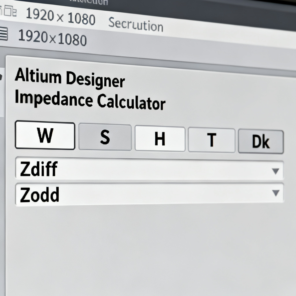
Altium Designer includes a built-in impedance calculator (Tools > Impedance Calculator). Steps:
- Select layer stack and target impedance (Zdiff).
- Input W, S, H, T, Dk.
- The tool computes Zdiff and Zodd. Adjust W and S iteratively to hit the target.
- For microstrip, consider solder mask effects: reduce trace width by 0.5–1 mil to compensate for increased capacitance.
Tip: Use the Field Solver option (if available in your license) for higher accuracy, especially for non-ideal geometries like trapezoidal traces.
Routing Differential Pairs for Impedance Consistency
Routing Guidelines
- Length Matching: Keep both traces equal length (within ±5 mil for high-speed signals). Use Interactive Length Tuning (Route > Interactive Length Tuning) to add serpentine sections.
- Symmetry: Maintain constant spacing (S) along the entire route. Avoid abrupt changes in width or spacing.
- Via Transitions: Minimize vias; when unavoidable, use ground vias adjacent to signal vias to maintain return path continuity. For differential vias, keep them close and symmetric.
- Avoid 90° Corners: Use 45° chamfers or arcs for corners to reduce impedance discontinuities.
Using the Differential Pair Routing Tool
- Select Route > Interactive Differential Pair Routing.
- Click on the first net of the pair; the tool automatically routes both traces with defined spacing.
- During routing, hold Ctrl to toggle between 45° and arc corners.
- Use Shift+Space to cycle through routing modes (e.g., push, hug, ignore obstacles).
Managing Impedance Discontinuities
- Neck-downs: When passing through tight component pads (e.g., BGA), ensure the neck-down length is minimal (< 100 mil) and width is not reduced below the calculated minimum.
- Return Path: Always provide a continuous ground plane beneath the differential pair. Avoid splits in the plane; if unavoidable, bridge with stitching capacitors.
- Solder Mask: For microstrip, apply solder mask only where needed; otherwise, leave exposed copper to maintain controlled impedance.
Validating Differential Pair Impedance
Using Altium Designer’s Signal Integrity Simulator
- Go to Tools > Signal Integrity.
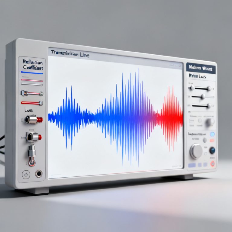
- Select the differential pair nets and run a Reflection or Crosstalk simulation.
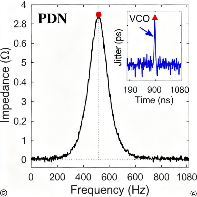
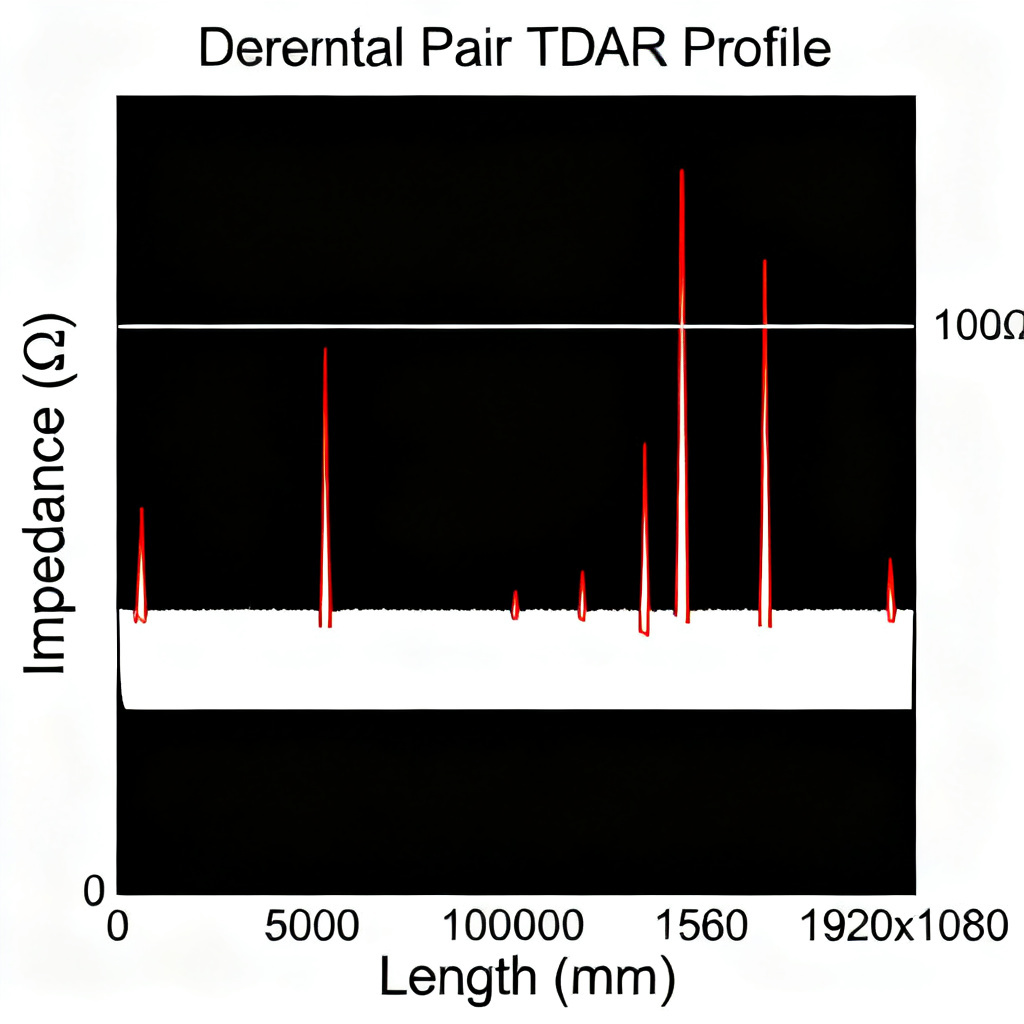
- Analyze the Impedance Profile: A flat impedance curve (e.g., 100Ω ±5Ω) indicates good control. Spikes indicate discontinuities.
- Use TDR (Time Domain Reflectometry) simulation to visualize impedance changes along the trace.
Exporting for 3D EM Simulation
For complex geometries (e.g., vias, connectors), export the PCB layout to external tools like Ansys HFSS or CST:
- Go to File > Export > STEP or ODB++.
- Import into the EM simulator and define port excitations at the differential pair endpoints.
- Run S-parameter simulation to validate Zdiff up to the target frequency (e.g., 10 GHz for PCIe Gen4).
Manufacturing Feedback and Coupon Testing
- Impedance Coupons: Add test coupons (e.g., 6-inch long traces) on the PCB panel. Request the manufacturer to measure Zdiff using a TDR and provide a report.
- Gerber Review: Ensure the Gerber files include impedance control notes (e.g., “Controlled impedance: 100Ω ±10% for differential pairs on Layer 1 and Layer 3”).
- Common Issues: If measured Zdiff is low, increase spacing; if high, decrease spacing or adjust width.
Best Practices for B2B PCB Manufacturing
Communicating with Your PCB Fabricator
- Provide a Stackup Table with target impedance, tolerance, and test method.
- Specify Material Grade (e.g., FR4 Tg 170°C for high-speed, or Rogers 4350B for RF).
- Request Impedance Control Certificate for each batch.
Common Pitfalls and Solutions
- Issue: Zdiff varies due to etching tolerance.
Solution: Use compensated design rules (e.g., target 100Ω ±8% to account for ±0.5 mil etching variation). - Issue: Solder mask thickens on microstrip, lowering impedance.
Solution: Request solder mask defined (SMD) pads for critical pairs, or use maskless areas. - Issue: Via stubs cause resonance.
Solution: Back-drill vias (remove stub length) for signals above 5 GHz.
Cost-Effective Impedance Control
- For standard FR4, use wider traces (e.g., 8 mil width) to relax manufacturing tolerances.
- Limit the number of impedance values (e.g., only 100Ω and 50Ω) to reduce setup costs.
- Use symmetrical stripline for inner layers to improve yield.
FAQ
What is differential pair impedance design in Altium Designer?
Differential pair impedance design in Altium Designer is the process of defining layer stack, routing rules, and validation methods to achieve target Zdiff for high-speed signals like USB or PCIe.
How do I set up differential pair impedance in Altium Designer?
Use the Layer Stack Manager to define materials, create differential pair net classes, set impedance rules in the PCB Rules Editor, and calculate trace geometry using the built-in Impedance Calculator.
What are common differential pair impedance targets?
Common targets include 100Ω for HDMI/Ethernet/LVDS, 90Ω for USB, and 85Ω for PCIe Gen3/4. Altium Designer supports all these via user-defined rules.
How do I validate differential pair impedance after routing?
Use Altium Designer’s Signal Integrity Simulator for TDR analysis, export to 3D EM tools for S-parameter validation, and request impedance coupon testing from your fabricator.
Why is differential pair impedance important for high-speed PCB?
Controlled differential pair impedance minimizes signal reflections, jitter, and EMI, ensuring reliable data transmission in protocols like PCIe, USB, and HDMI.
| Protocol | Target Zdiff (Ω) | Typical Stackup |
|---|---|---|
| USB 2.0/3.0 | 90 | Microstrip |
| HDMI | 100 | Microstrip/Stripline |
| PCIe Gen3/4 | 85 | Stripline |
| Ethernet | 100 | Microstrip |
| LVDS | 100 | Microstrip/Stripline |