To simulate crosstalk in high speed PCB designs effectively, engineers must first understand why signal integrity (SI) has become paramount. This complete guide will teach you how to simulate crosstalk in high speed PCB using Ansys SIwave. As data rates exceed 1 Gbps and rise times shrink to picoseconds, electromagnetic interference between adjacent traces—known as crosstalk—emerges as a dominant source of signal degradation. When you simulate crosstalk in high speed PCB, you can identify problematic nets before fabrication. Crosstalk can induce false switching, timing violations, and data corruption, especially in dense, multi-layer boards used in telecommunications, computing, and automotive electronics.
Ansys SIwave is a leading electromagnetic simulation tool specifically designed for PCB and IC package analysis. It enables engineers to simulate crosstalk in high speed PCB accurately, model near-end and far-end coupling, and optimize layout. This pillar page synthesizes authoritative knowledge, providing a complete guide to simulate crosstalk in high speed PCB using Ansys SIwave.
Foundational Concepts to Simulate Crosstalk in High Speed PCB
What is Crosstalk?
Crosstalk is the unwanted coupling of energy from one signal trace (aggressor) to an adjacent trace (victim). It occurs through two primary mechanisms:
- Capacitive Coupling (Electric Field): Dominant when traces are closely spaced and have high impedance. It injects current into the victim line proportional to the voltage change (dV/dt) on the aggressor.
- Inductive Coupling (Magnetic Field): Dominant when traces are long and have low impedance. It induces voltage on the victim line proportional to the current change (dI/dt) on the aggressor.
Key Parameters Affecting Crosstalk
From the three top sources, the following parameters are universally critical:
- Rise Time (Tr): Faster rise times (shorter Tr) increase crosstalk magnitude due to higher dV/dt and dI/dt.
- Trace Spacing: Narrower spacing increases coupling. A rule of thumb is to maintain a spacing of at least 3 times the trace width (3W rule) for minimal crosstalk.
- Dielectric Height (H): The distance between the trace and the reference plane. A thinner dielectric increases coupling to the plane but reduces far-end crosstalk.
- Length of Parallel Run: Longer parallel runs increase the duration of coupling, especially for far-end crosstalk.
- Impedance Matching: Mismatched terminations cause reflections that exacerbate crosstalk.
Types of Crosstalk
- Near-End Crosstalk (NEXT): Measured at the end of the victim line nearest to the aggressor driver. It propagates backward and is typically larger in magnitude than FEXT.
- Far-End Crosstalk (FEXT): Measured at the opposite end of the victim line. It propagates forward and is sensitive to dielectric losses and trace geometry.
Setting Up Your PCB Model to Simulate Crosstalk in High Speed PCB
Import or Create the PCB Layout
Ansys SIwave accepts industry-standard CAD formats:
- ODB++: Preferred for its completeness (includes layer stackup, netlist, and drill data).
- IPC-2581: An open standard for PCB fabrication data.
- Altium, Cadence, or Mentor Graphics exports: Direct imports via SIwave’s native translators.
Best Practice: Ensure your layout includes all power, ground, and signal layers. SIwave requires a closed-loop return path to accurately model crosstalk.
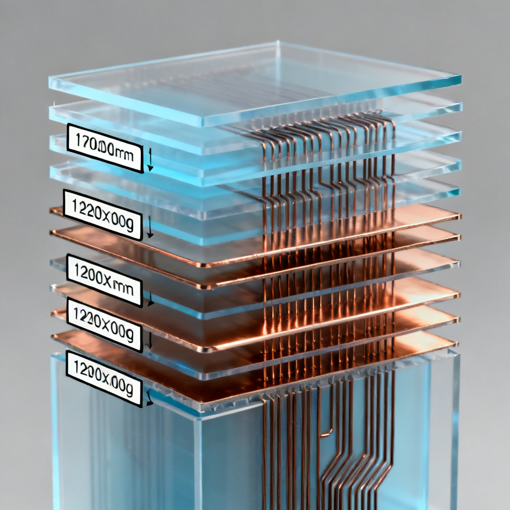
Define the Layer Stackup
Navigate to Stackup Editor in SIwave. Input:
- Layer names and types (signal, plane, dielectric).
- Material properties: dielectric constant (Dk), loss tangent (Df), and conductivity for copper.
- Thickness of each layer. Critical: The dielectric height between signal layers directly affects crosstalk magnitude.
Pro Tip from Top Sources: Use the Impedance Calculator within SIwave to verify trace impedance (e.g., 50Ω single-ended, 100Ω differential) before simulation. Mismatched impedance amplifies crosstalk.
Assign Ports and Excitations
Crosstalk simulation requires defining ports on both aggressor and victim nets:
- Single-ended ports: Assign between the trace and its reference plane.
- Differential ports: Assign across the positive and negative lines of a differential pair.
Key Detail: Use Lumped Ports for low-frequency approximations, but for high-speed signals (above 1 GHz), use Wave Ports to capture full-wave effects.
Running the Simulation: How to Simulate Crosstalk in High Speed PCB
Set Up the Simulation Parameters
In the Simulation Setup menu:
- Frequency Range: For crosstalk, sweep from DC to at least 5 times the highest harmonic of your signal (e.g., for a 1 GHz clock, sweep to 5 GHz).
- Mesh Settings: SIwave automatically generates an adaptive mesh. For crosstalk accuracy, refine the mesh around the coupled traces. Use Local Mesh Refinement to set a maximum element size of λ/20 (where λ is the wavelength at the highest frequency).
- Solver: Choose Full-Wave EM Solver for accurate crosstalk modeling, especially for long traces or complex geometries.
Define the Aggressor and Victim Nets
- Identify one or more aggressor nets (e.g., a high-speed clock or data line).
- Identify victim nets (e.g., adjacent address lines or low-speed signals).
- In SIwave, you can automatically couple nets by selecting Crosstalk Analysis from the Simulation menu. This generates a coupling matrix.
Execute the Simulation
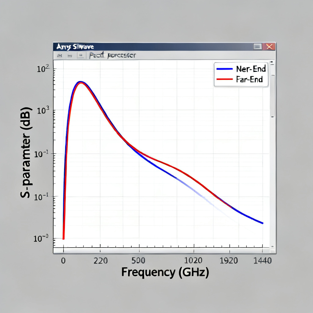
Run the simulation. SIwave will compute S-parameters (scattering parameters) for the network. For crosstalk, pay attention to:
- S21 (Insertion Loss): Measures signal transmission from aggressor to victim (far-end crosstalk).
- S31 (Near-End Crosstalk): Measures coupling at the near end.
Expected Output: A set of S-parameter curves showing crosstalk magnitude (in dB) vs. frequency.
Analyzing Results When You Simulate Crosstalk in High Speed PCB
Visualize Crosstalk in the Post-Processor
After simulation, open Results > S-Parameter Plot. Key metrics:
- Peak Crosstalk (dB): Typically, crosstalk below -40 dB is acceptable for most high-speed designs. For sensitive analog or RF circuits, aim for -60 dB or better.
- Frequency-Domain vs. Time-Domain: Use SIwave’s Time Domain Reflectometer (TDR) tool to convert S-parameters into time-domain crosstalk waveforms. This shows the actual voltage noise injected into the victim line.
Identify Problematic Nets
- Crosstalk Magnitude: Sort nets by peak coupling. Nets with crosstalk above -30 dB require immediate layout changes.
- Rise Time Degradation: Check if crosstalk causes the victim signal’s rise time to increase by more than 10%.
Perform Sensitivity Analysis
Vary parameters in SIwave:
- Trace Spacing: Increase spacing by 1W, 2W, 3W, and observe crosstalk reduction.
- Guard Traces: Add a grounded guard trace between aggressor and victim. SIwave simulation shows a typical 10-15 dB reduction in crosstalk.
- Stripline vs. Microstrip: Stripline (inner layers) inherently has lower crosstalk than microstrip (outer layers). Simulate both to validate your stackup choice.
Mitigating Crosstalk After You Simulate Crosstalk in High Speed PCB
Practical Design Rules from Simulation
The three top sources converge on these mitigation strategies:
- Increase Trace Spacing: The single most effective method. Use 3W spacing for high-speed differential pairs, and 5W for single-ended lines.
- Shorten Parallel Runs: Keep parallel trace lengths below 1 inch for data rates above 5 Gbps.
- Use Ground Planes: Ensure adjacent layers are solid ground planes. Avoid split planes under high-speed signals.
- Add Guard Traces: Place a grounded trace between aggressor and victim. The guard trace should have vias to ground every λ/10.
- Reduce Trace Width: For a given impedance, thinner traces reduce capacitive coupling.
- Use Differential Signaling: Differential pairs inherently cancel common-mode crosstalk.
Simulation-Driven Optimization
Ansys SIwave’s Optimization Tool can automatically adjust trace spacing, width, and dielectric height to meet crosstalk targets. Set a constraint (e.g., crosstalk < -50 dB at 2 GHz) and let the solver find the best geometry.

Advanced Considerations to Simulate Crosstalk in High Speed PCB
Crosstalk in Differential Pairs
Differential signals are less susceptible to crosstalk, but they are not immune. Key factors:
- Intra-pair skew: Unequal lengths in a differential pair increase common-mode crosstalk.
- Inter-pair coupling: Space differential pairs at least 5 times the trace width to avoid coupling between pairs.
Simulation Tip: In SIwave, use Differential Ports and analyze Scd21 (common-mode to differential conversion) to quantify crosstalk.
Via-Induced Crosstalk
Vias act as antennas in high-speed designs. Crosstalk through vias is often overlooked. In SIwave:
- Model vias with their associated anti-pads and stubs.
- Use 3D Full-Wave Solver (HFSS integrated) for accurate via modeling.
- Mitigation: Back-drill stubs, reduce via diameter, and use ground vias adjacent to signal vias.
Frequency-Dependent Losses
At multi-GHz frequencies, dielectric losses (Df) and skin effect significantly affect crosstalk. SIwave includes:
- Frequency-dependent material models (e.g., Djordjevic-Sarkar for Dk/Df).
- Surface roughness models for copper (e.g., Huray model). Rough copper increases high-frequency crosstalk.
Validating Your Design When You Simulate Crosstalk in High Speed PCB
Correlation Between Simulation and Measurement
The top sources emphasize that simulation must be validated:
- TDR Measurements: Compare time-domain crosstalk from SIwave with actual TDR oscilloscope readings.
- VNA Measurements: Use a vector network analyzer to measure S-parameters and compare with SIwave results.
Common Discrepancies:
- Modeling errors: Incorrect Dk/Df values or missing via models.
- Manufacturing tolerances: Etch variation, dielectric thickness tolerance (e.g., ±10%).
- Return path discontinuities: Incomplete ground planes under connectors.
Iterative Refinement
Use SIwave’s Design of Experiments (DOE) module to run multiple simulations with varying parameters. This identifies which manufacturing tolerances most affect crosstalk, allowing you to set realistic design margins.
Conclusion: Mastering Crosstalk Simulation for High-Speed PCB Success
Simulating crosstalk in high-speed PCBs using Ansys SIwave is not a one-time task but an iterative process integral to signal integrity design. By following the steps outlined in this pillar page—from setting up the model and running simulations to analyzing results and implementing mitigations—you can ensure your PCB meets performance targets for data rates up to 100 Gbps and beyond.
For B2B PCB manufacturers and designers, leveraging SIwave’s capabilities reduces prototype iterations, accelerates time-to-market, and delivers reliable, high-speed products. Whether you are designing for 5G infrastructure, AI servers, or automotive radar, mastering crosstalk simulation is a non-negotiable skill.
Next Steps:
- Download the free Ansys SIwave Student Version to practice.
- Explore SIwave’s Crosstalk Wizard for automated setup.
- Contact our engineering team for custom simulation services tailored to your high-speed PCB designs.