High-speed PCBs are the foundational component for high-frequency, high-bandwidth, and high-data-rate electronic systems across global industrial, telecom, automotive, and aerospace industries. Unlike conventional standard circuit boards, high-speed printed circuit boards require strict control over signal integrity (SI), controlled impedance, low-loss substrates, optimized layer stack-up, crosstalk reduction, and EMI suppression.
This ultimate guide is created for international hardware engineers, PCB designers, industrial procurement managers, and overseas B2B buyers. It combines professional industry theory, real-world design best practices, and high-speed PCB manufacturing expertise. Every key concept is explained with clear logic, balancing technical depth and easy understanding. You will learn high-speed circuit principles, common SI issues, material selection, layout guidelines, DFM rules, testing standards, and industrial applications to eliminate design flaws, signal loss, and mass production risks for your high-speed projects.
1. Introduction: What Is High-Speed PCB & Signal Integrity
With the rapid iteration of global high-end electronics, high-speed interfaces such as PCIe Gen4/Gen5, 10G/25G Ethernet, 56G PAM-4, and 112Gbps SerDes have become mainstream in servers, 5G telecom equipment, smart vehicles, and high-precision industrial devices.
Traditional regular FR-4 PCBs cannot support ultra-fast data transmission, resulting in waveform distortion, signal attenuation, timing errors, system instability, and equipment downtime.
A High-Speed PCB is defined as a circuit board designed for operating frequencies above 50MHz, signal rise time lower than 1ns, and data transmission rates over 1Gbps.
Signal Integrity (SI) refers to the ability of electrical signals to transmit completely, stably, and accurately without interference or distortion along the PCB trace.
For overseas industrial buyers and engineering teams, high-speed PCB quality directly determines product reliability, certification compliance, and long-term service life. Professional design and high-quality manufacturing are essential for export electronic products.
2. Core Principles & Definition Standards of High-Speed Circuits
Many industry professionals confuse high-frequency PCB with high-speed PCB. The core judgment is not only frequency, but signal rise time, transmission path characteristics, and electromagnetic wave propagation.
2.1 Key High-Speed Judgment Criteria
- Operating frequency: above 50MHz
- Data rate: ≥ 1Gbps
- Short signal rise time: less than 1ns
- Critical length calculation directly affects signal quality
2.2 Basic Transmission Theory
High-speed signals do not simply flow as current; they propagate as electromagnetic waves between copper traces and dielectric substrates. Any discontinuity in line width, dielectric thickness, reference plane, or layer structure will break electromagnetic balance and cause irreversible signal degradation. This fundamental difference separates high-speed PCB design from ordinary circuit board design.
3. Common Signal Integrity (SI) Issues & Root Causes
All high-speed PCB design specifications are developed to solve typical SI failures that frequently occur in mass production:
- Signal Reflection: Caused by impedance discontinuity, sudden trace changes, poor via design, and broken reference planes, leading to waveform distortion and logic errors.
- Crosstalk Interference: Electromagnetic coupling between adjacent parallel traces, triggered by long parallel routing, insufficient spacing, and lack of grounding shielding.
- Insertion Loss & Signal Attenuation: Skin effect, copper loss, and dielectric loss weaken high-speed signals, especially in 25Gbps+ ultra-high-speed scenarios.
- Skew & Timing Mismatch: Unbalanced differential line length and inconsistent routing paths cause transmission delay differences.
- Power & Ground Noise: Imperfect power integrity and incomplete ground planes introduce high-frequency noise.
- EMI Radiation: Unreasonable loop design leads to electromagnetic leakage, affecting EMC certification for export products.
4. Controlled Impedance: The Core of High-Speed PCB Performance
Controlled impedance is the most critical technical indicator of high-speed PCB and the top concern for international engineering purchasers. All high-speed signal lines require precise impedance matching for specific industry interfaces.
4.1 Industry Standard Impedance Values
- Single-ended signal: 50Ω standard
- General differential pair: 100Ω
- PCIe interface: 85Ω differential impedance
- USB & HDMI high-speed: 90Ω differential impedance
- DDR memory circuit: 40Ω–60Ω adjustable impedance
4.2 Main Factors Affecting Impedance
Trace width, dielectric thickness, substrate Dk (dielectric constant), Df (dissipation factor), copper thickness, and microstrip/stripline structure.
4.3 Manufacturing Tolerance Grade
Premium high-speed PCB manufacturers support ±3% high-precision impedance control, while standard factories only provide ±5% tolerance. For 10Gbps+ high-speed equipment, ±3% precision is mandatory for stable long-term operation.
5. High-Speed PCB Layer Stack-Up Design & Structural Optimization
A scientific layer stack-up is the foundation of stable signal integrity. It applies to 4-layer, 6-layer, 8-layer, and multi-layer high-speed PCB solutions for global industrial projects.
5.1 Core Stack-Up Design Principles
- High-speed signal layers must be tightly coupled with complete ground planes for continuous return paths.
- Separate high-speed signal layers from power layers to avoid noise coupling.
- Adopt alternating arrangement of signal / ground / power layers to reduce crosstalk.
- Minimize layer switching and via usage for critical high-speed traces.
5.2 Common Industrial Stack-Up Solutions
- 4-layer high-speed PCB: Signal – GND – Power – Signal
- 6-layer high-speed PCB: Signal – GND – Signal – Power – GND – Signal
- 8-layer high-end high-speed PCB: Dual ground plane isolation, dedicated differential shielding for server and 5G devices
Complete ground plane coverage stabilizes impedance, suppresses crosstalk, and reduces EMI radiation effectively.
6. Differential Pair Routing Rules & Engineering Best Practices
Differential pair transmission is the mainstream solution for modern high-speed interfaces, widely used in Ethernet, PCIe, HDMI, SATA, and high-speed serial buses.
6.1 Strict Design Guidelines
- Control length mismatch within ±5mil
- Maintain consistent trace width, spacing, and symmetric routing
- Route on the same layer and avoid cross-layer switching
- Keep away from high-power traces, analog circuits, and dense via arrays
6.2 Advantages of Differential Signals
Powerful anti-interference capability, common-mode noise suppression, low electromagnetic radiation, and stable transmission performance, ideal for 10Gbps and above ultra-high-speed systems.
7. Crosstalk Reduction, Signal Reflection & Termination Solutions
7.1 Practical Crosstalk Suppression Methods
- Widen spacing between high-speed traces and adjacent lines
- Limit parallel routing length of coupled signals
- Add ground guard traces in dense high-speed wiring areas
- Use stripline structure with double-sided ground shielding
7.2 Impedance Termination Technology for Reflection
Impedance matching termination eliminates signal reflection fundamentally:
- Series termination: Suitable for short-distance high-speed signals
- Parallel termination: Stabilizes signal voltage level
- AC coupling termination: Protects high-speed chip ports and isolates DC bias
Designers can select targeted termination solutions based on interface type, transmission distance, and operating speed.
8. High-Speed Via Design Optimization: Anti-Stub & HDI Technology
Traditional through-hole vias create residual stubs, break impedance continuity, and cause severe high-frequency signal loss. High-speed PCB requires fully optimized via design.
8.1 High-Speed Via Optimization Standards
- Reduce via quantity for critical high-speed signals
- Replace standard through holes with blind vias, buried vias, and HDI microvias
- Eliminate via stubs via back-drilling technology
- Configure adjacent ground vias to optimize high-speed return current
Back-drilling and HDI microvia processes are standard configurations for server PCBs, automotive high-speed electronics, and 5G communication hardware.
9. Low-Loss PCB Materials: Types, Parameters & Selection Guide
PCB substrate material determines the upper limit of high-frequency signal loss. Different data rate applications require matched low-Dk and low-Df materials.
9.1 Mainstream High-Speed PCB Materials
- Enhanced Low-Loss FR-4Cost-effective, suitable for 1Gbps–3Gbps mid-speed industrial control and general communication devices.
- Rogers High-Frequency MaterialsModels: Rogers 4003C, 4350BUltra-low Dk/Df, excellent high-frequency stability, ideal for 5G base stations and RF high-speed equipment.
- Megtron High-Speed SeriesMegtron 6 / Megtron 7, ultra-low transmission loss, customized for 25Gbps–112Gbps data center and server hardware.
- Isola & Tachyon Ultra-Loss SubstratesFor PAM-4 ultra-high-speed signals, aerospace, and high-reliability premium industrial equipment.
9.2 Material Selection Reference
- 1–10Gbps: Modified low-loss FR-4
- 10–56Gbps: Megtron series or Rogers hybrid laminate
- 56Gbps and above: Imported ultra-low-loss specialty dielectric materials
10. Power Integrity (PI) and Signal Integrity Co-Design
Signal integrity cannot work independently without stable power integrity. Power noise and fragmented ground planes directly interfere with high-speed signals.
10.1 Key PI Design Requirements
- Maintain complete, unbroken ground planes
- Arrange high-density decoupling capacitors near high-speed ICs
- Avoid sudden power trace width changes and branch circuits
- Reasonably partition analog ground, digital ground, and high-speed ground
Early co-design of SI and PI in layout stages is critical for multi-layer high-speed PCB success.
11. EMI Control & EMC Compliance for Export-Grade High-Speed PCB
High-speed high-frequency signals easily generate electromagnetic radiation, causing EMC test failures and blocking market access for export products.
11.1 EMC Optimization Measures
- Complete ground plane shielding to reduce electromagnetic leakage
- Centralized layout of high-speed sensitive circuits
- Add edge grounding via arrays for board-level shielding
- Minimize high-speed loop area to weaken antenna radiation effects
All our high-speed PCB designs follow international EMC standards to meet EU, North American, and global industrial certification requirements.
12. High-Speed PCB Manufacturing Process & DFM Guidelines
Many perfect high-speed design plans fail in mass production due to ignored DFM rules. As a professional export high-speed PCB supplier, we combine design feasibility and manufacturing capability.
12.1 Core Advanced Manufacturing Technologies
- ±3% high-precision controlled impedance production
- Back-drilling anti-stub processing
- HDI blind & buried via fabrication
- Rogers / low-loss material hybrid lamination
- High-layer count, high-reliability pressing technology
12.2 DFM Tips for Global Buyers
- Reserve process margin for differential pairs and impedance traces
- Clearly define impedance tolerance, material brand, and special process requirements in procurement documents
- Avoid ultra-fine lines and ultra-small spacing beyond industrial production limits
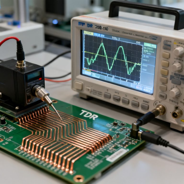
13. Professional Testing & Quality Control for High-Speed PCB
Authoritative testing and full quality inspection are essential to verify signal integrity performance before shipment.
13.1 Core Testing Items
- TDR impedance testing for actual impedance verification
- S-parameter testing: insertion loss, return loss analysis
- Layer pressing inspection and appearance quality check
- High temperature & humidity reliability aging test
- Insulation and conductivity performance testing
We provide complete test reports and support third-party inspection to meet global industrial customer quality standards.
14. Global Industrial Applications of High-Speed PCB
High-speed PCBs are widely used in high-end export industries worldwide:
- Telecommunications: 5G/6G base stations, optical modules, high-frequency routing equipment
- Data Center & AI: High-performance servers, GPU mainboards, high-speed backplanes
- Automotive Electronics: Autonomous driving control boards, vehicle Ethernet
- Industrial & Medical: High-precision testing instruments, medical high-speed imaging devices
- Aerospace: High-reliability high-frequency control circuits
15. Frequently Asked Questions (FAQ)
Q1: What is the difference between high-speed PCB and high-frequency PCB?
A1: High-frequency PCB focuses on radio frequency performance, while high-speed PCB centers on signal integrity, impedance control, and data transmission stability. Most high-end devices require both high-speed and high-frequency capabilities.
Q2: What is the most important parameter for high-speed PCB customization?
A2: Controlled impedance tolerance, substrate Dk/Df value, layer stack-up structure, and via processing technology are the four core parameters that determine SI performance.
Q3: Can you provide custom controlled impedance PCB production?
A3: Yes. We support customized impedance from 20Ω to 120Ω with ±3% high-precision tolerance and provide professional impedance calculation and DFM review.
Q4: What low-loss PCB materials do you supply?
A4: We supply low-loss FR-4, Rogers 4003C/4350B, Megtron 6/7, Isola, and Tachyon series materials for different high-speed rate requirements.
Q5: Do you offer free design consultation and quotation for overseas buyers?
A5: Absolutely. Our professional engineering team provides free DFM checking, high-speed design suggestions, and exclusive factory direct quotes for global customers.
16. Final Summary & Custom High-Speed PCB Inquiry
This ultimate guide fully covers high-speed PCB basic knowledge, signal integrity principles, impedance design, layer stack-up, differential routing, crosstalk control, via optimization, low-loss material selection, EMI design, manufacturing technology, testing standards, and industry applications.
High-speed PCB is highly customized B2B industrial product. Stable signal integrity, reasonable cost, reliable lead time, and export-grade quality depend on professional design and experienced high-speed PCB manufacturer.
Whether you are an electronic engineer needing technical support, an industrial procurement manager looking for reliable high-speed PCB suppliers, or a company with high-speed circuit project demands, we provide one-stop export solutions:
✅ Free high-speed PCB DFM audit & technical consulting
✅ Custom controlled impedance PCB manufacturing
✅ Multi-layer, HDI, back-drilling, mixed material lamination service
✅ Export-grade quality control & complete test reports
✅ Fast global delivery and competitive factory pricing
If you have PCB design files, technical parameters, sample demands, or bulk procurement plans, contact our team today to get your free custom quotation and professional high-speed signal integrity solution.