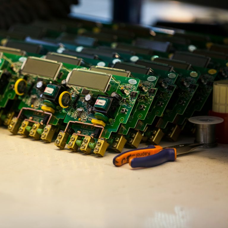
Back drilling is a critical controlled-depth secondary drilling process for modern high-speed PCBs. It eliminates unused via copper stubs that cause signal reflection, electromagnetic resonance, jitter degradation and eye diagram closure.
With the rapid upgrade of PCIe 4.0/5.0, 100G Ethernet, 112G PAM4, DDR5 and AI server backplane designs, traditional full-through vias can no longer meet high-speed integrity requirements.
This full pillar guide explains what back drilling is, the mechanism of via stub interference, working principle, critical manufacturing parameters, standard DFM design rules, comparison with blind and buried vias, industry application scenarios, professional checklist and frequently asked questions.
The PCB Manufacturing & Testing Guidelines, which covers all manufacturing processes from prototype to mass production, complements this back drilling-focused guide. Understanding back drilling high speed pcb is essential for modern high-speed design.
Table of Contents
- 1. What Is Back Drilling in High-Speed PCB?
- 2. The Via Stub Problem: How Unremoved Stubs Ruin High-Speed Signals
- 3. Resonance Frequency Formula & Data Rate Impact Grading
- 4. How PCB Back Drilling Works: Full Process Principle
- 5. Back Drilling Key Manufacturing Parameters: Standard vs Advanced Specs
- 6. Essential Back Drilling DFM Design Rules for High-Speed Layout
- 7. Back Drilling vs Blind Vias vs Buried Vias: Cost, Performance & Application
- 8. Industry Application Scenarios: PCIe, 100G, 112G PAM4 & More
- 9. Professional Back Drilling Design & Manufacturing Checklist
- 10. Key Takeaways
- 11. Back Drilling FAQ
- 12. Get Free DFM Evaluation & Custom Back Drilling Support
What Is Back Drilling in High-Speed PCB?
Back drilling, also named Controlled Depth Drilling (CDD), is a specialized secondary PCB manufacturing process. It drills away the redundant unused copper barrel segment of standard through-hole vias.
This leaves only the necessary conductive part for signal layer connection.
In conventional PCB fabrication, through-hole vias penetrate the entire board stackup. When a via only connects partial inner layers, the extra copper barrel extending beyond the last connected layer forms a redundant idle section — known as a via stub.
Back drilling precisely removes this stub from the reverse side of the PCB without damaging valid signal interconnections.
The core purpose of implementing back drilling high speed pcb includes eliminating via stub induced signal reflection, suppressing high-frequency electromagnetic resonance, reducing jitter, and ensuring stable transmission for 10Gbps+ signals.
This process has become a baseline requirement for data center switches, AI computing motherboards, and high-speed backplanes.
For detailed via stub analysis that back drilling addresses, the High-Speed PCB Via Design Guide provides comprehensive coverage of via-related signal integrity issues.
The Via Stub Problem: How Unremoved Stubs Ruin High-Speed Signals
A via stub is essentially an extra idle conductive transmission line inside the PCB stackup. Unlike functional signal traces, stubs do not carry valid signals. They act as natural resonant cavities at high frequencies.
The main negative impacts of unprocessed via stubs include:
- Signal Reflection: Sudden impedance change at the stub end causes signal reflection, interfering with original transmission waveforms.
- Quarter-Wave Resonance: Stubs form resonant structures, creating fixed-frequency notch attenuation that directly attenuates signal amplitude within the working bandwidth.
- Parasitic Capacitance & Inductance: Extra copper barrel introduces parasitic effects, destroying controlled impedance design of high-speed differential pairs.
- EMI Degradation: Resonant radiation increases electromagnetic interference, failing EMC compliance tests.
- Differential Phase Skew: Asymmetric stub length on differential pairs breaks common-mode rejection capability, leading to serious eye diagram shrinkage.
The higher the signal transmission rate, the more sensitive the circuit becomes to stub length.
Low-speed designs can ignore stubs. However, 56Gbps and 112G PAM4 ultra-high-speed designs are extremely vulnerable to even short residual stubs.
Resonance Frequency Formula & Data Rate Impact Grading
The resonant notch frequency caused by via stubs follows a clear physical formula:
f ≈ 1 / (4 × Stub Length × Signal Propagation Velocity)
From the formula: the longer the via stub, the lower the resonant frequency. Longer stubs easily fall into the operating frequency range of high-speed interfaces. This causes fatal signal attenuation.
| Signal Data Rate | Stub Impact Level | Back Drilling Requirement |
|---|---|---|
| ≤5Gbps | Negligible | Not required |
| 5Gbps – 10Gbps | Mild interference | Optional, cost-dependent |
| 10Gbps – 25Gbps | Obvious resonance & reflection | Strongly recommended |
| 25Gbps – 56Gbps | Severe signal distortion | Mandatory |
| 56Gbps – 112Gbps (PAM4) | Fatal to signal integrity | Strictly enforced |
This grading standard is widely adopted in IPC design norms and PCIe/100G Ethernet specifications. It helps designers determine when back drilling high speed pcb becomes mandatory for their projects.
How PCB Back Drilling Works: Full Process Principle
Back drilling follows a standardized, precision-controlled manufacturing workflow. It retains valid connections while trimming redundant stubs.
Standard Through-Hole Drilling & Plating: Complete full-stack drilling and electroplating to form continuous copper via barrels through all PCB layers.
Reverse Side Controlled Depth Secondary Drilling: Manufacturers use high-precision CNC drilling equipment with a larger diameter drill bit than the original via hole. They drill from the board’s reverse side to ensure complete removal of surrounding redundant copper without hurting inner substrate.
Precision Depth Termination: Drilling stops exactly at the predefined reference layer. This perfectly reserves electrical connections between target signal layers.
Final Residual Stub Control: After back drilling, the residual via stub length is strictly controlled at 5–10mil. Advanced ultra-high-speed designs target 5mil minimum stub to suppress resonance to the lowest level.
Back Drilling Key Manufacturing Parameters: Standard vs Advanced Specs
Manufacturing parameters determine back drilling yield, precision and final signal integrity performance. Factories divide specs into standard grade and advanced grade for different layer counts and speed requirements.
| Key Parameter | Standard Specification | Advanced Specification |
|---|---|---|
| Supported Back Drilling Layers | 1–6 layers | 8 layers and above |
| Drilling Depth Tolerance | ±0.1mm | ±0.05mm |
| Minimum Residual Stub Length | 10mil | 5mil |
| Minimum Safe Trace Width Near Vias | 4mil | 3mil |
Depth tolerance is the most critical parameter for back drilling high speed pcb. Loose tolerance leads to over-drilling or under-drilling. 56G/112G PAM4 designs must adopt ±0.05mm high precision.
The DFM Rules for High-Speed PCB, which covers line width, spacing, and via design rules, provides additional manufacturing guidelines that complement these back drilling parameters.
Essential Back Drilling DFM Design Rules for High-Speed Layout
To ensure manufacturability, stable impedance and differential signal performance, all high-speed PCB layouts must follow unified back drilling high speed pcb DFM design rules.
Clear Start & End Layer Definition
Designers must explicitly mark the exact start layer and stop layer for every back-drilled via in stackup documents. Ambiguous layer definition will cause wrong drilling depth. This results in open circuits or untrimmed long stubs. All PCIe, 100G and 112G differential vias need independent layer labeling.
Maintain Minimum Safety Clearance
Keep at least 4mil spacing between back-drilled via wall and adjacent traces, pads and copper planes. Insufficient clearance risks copper short circuit, substrate delamination and drilling burrs.
Symmetric Back Drilling for Differential Pairs
Both vias of a high-speed differential pair must adopt symmetric back drilling with identical residual stub length. Asymmetric stubs introduce phase skew, damage common-mode rejection and severely degrade eye diagram quality.
Avoid Back Drilling Near Sensitive High-Speed Traces
Arrange back-drilled vias away from critical impedance-controlled traces. This prevents drilling mechanical stress and copper residue from affecting signal stability.
Accurate impedance control is essential for high-speed designs using back drilling. The Impedance Matching Ultimate Guide explains the relationship between via stubs, impedance discontinuity, and signal reflection.
Back Drilling vs Blind Vias vs Buried Vias: Cost, Performance & Application
Designers have two mainstream solutions to eliminate via stubs: back drilling and sequential lamination blind/buried vias. Each has obvious advantages in cost, performance and applicable scenarios.
| Solution | Production Cost | Signal Performance | Layout Density | Best Application |
|---|---|---|---|---|
| Back Drilling | Low (Cost increase ~10–15%) | Good | Medium | 10Gbps – 56Gbps mass production PCBs |
| Blind / Buried Vias | High (Cost increase ~50–100%) | Excellent | High (HDI support) | 56G–112G PAM4, HDI high-density boards, aerospace |
Back drilling is based on traditional through-hole process with no complex multi-time lamination. This makes it cost-effective for most 10–56Gbps commercial high-speed projects.
For more on HDI structures where blind/buried vias are used, the HDI PCB Manufacturing Guide provides detailed process information.
Industry Application Scenarios: PCIe, 100G, 112G PAM4 & More
Back drilling high speed pcb is standard configuration for all mainstream high-speed interface and high-end hardware products:
- PCIe 4.0 / 5.0 / 6.0: Graphics cards, AI accelerator cards, server mainboards
- 100G / 112G PAM4 Ethernet: Data center switches, optical transmission equipment, network backplanes
- DDR5 & High-Speed Memory Interface: High-performance computing motherboards
- AI Server & High-Speed Computing Backplane: Large-scale cluster hardware
- 5G / 6G Communication Base Station Boards: Radio frequency and high-speed signal carrier boards
- Aerospace & Industrial High-Reliability PCB: High-speed control and transmission modules
All above scenarios require strict back drilling parameter control and DFM rule compliance. This ensures they pass signal integrity, EMC and long-term reliability tests.
Professional Back Drilling Design & Manufacturing Checklist
- Mark all vias of 10Gbps+ differential pairs for mandatory back drilling
- Ensure back-drilled via areas keep 4mil safety clearance from nearby traces and copper
- Clearly specify depth tolerance and residual stub length in fabrication notes (standard 10mil / advanced 5mil)
- Verify symmetric back drilling setup for all differential pair vias
- Confirm your PCB supplier’s maximum supported layer count and back drilling precision capability
- Check stackup layer definition to avoid over-drilling or under-drilling errors
Key Takeaways
- Back drilling high speed pcb is the most cost-effective via stub removal process for high-speed PCBs, essential for 10Gbps+ signal design
- Via stub length directly determines resonant frequency; shorter residual stubs (5–10mil) guarantee high-speed signal integrity
- 10–25Gbps recommends back drilling; 25Gbps and above is mandatory; 56G–112G PAM4 requires advanced 5mil minimum stub and ±0.05mm depth tolerance
- Strictly follow DFM rules: clear layer definition, 4mil safety spacing, symmetric back drilling for differential pairs
- Back drilling balances low cost and good performance for 10–56Gbps mass production; blind/buried vias fit HDI and ultra-high-speed high-end scenarios
- Standardize checklist review before file release to avoid manufacturing rework and signal integrity failure
Back Drilling FAQ
Q1: What is the standard residual stub length after back drilling?
General commercial designs control 10mil residual stub; 56G/112G PAM4 advanced designs require 5mil minimal stub for optimal back drilling high speed pcb performance.
Q2: Is back drilling necessary for 10Gbps PCB?
10Gbps is the threshold; it is strongly recommended to adopt back drilling to avoid long-term signal instability and jitter issues.
Q3: What is the depth tolerance difference between standard and advanced back drilling?
Standard ±0.1mm, advanced high-precision ±0.05mm for thick stackup and ultra-high-speed interfaces.
Q4: Should differential pairs use symmetric back drilling?
Yes. Asymmetric stub length causes phase skew and damages differential signal performance — a critical rule in back drilling high speed pcb design.
Q5: Which is better: back drilling or blind buried via?
Choose back drilling for cost-sensitive 10–56Gbps projects; choose blind/buried vias for HDI density and 56G+ ultra-high-speed scenarios with sufficient budget.
Q6: Will back drilling increase PCB cost much?
Only a moderate increase of 10–15%, far lower than the cost of blind and buried vias, with excellent cost-performance for back drilling high speed pcb implementation.
Get Free DFM Evaluation & Custom Back Drilling Support
If you are designing high-speed PCBs for PCIe 5.0, 100G or 112G PAM4 applications, improper back drilling high speed pcb setup often leads to signal integrity failure, production rework and delayed project delivery.
We offer: Free back drilling DFM design review & risk assessment • Custom stackup design with matched back drilling layer definition • Parameter optimization for 5mil/10mil stub and depth tolerance • Professional manufacturing quotation and process solution customization
Submit your PCB design files and project requirements now, and get free technical consultation, design optimization suggestion and exclusive factory quotation within the shortest time.
About HighSpeedPCBs.com
We are a specialized PCB design and manufacturing service provider serving industrial, automotive, medical, and communications OEMs worldwide. Our expertise in back drilling high speed pcb ensures your high-speed designs achieve optimal signal integrity.
Complete manufacturing process documentation is available in the PCB Manufacturing & Testing Guidelines.
© 2026 HighSpeedPCBs.com — Professional High-Speed PCB Solutions