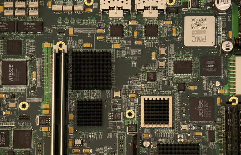
High-speed PCB design differs greatly from conventional circuit boards, requiring strict signal integrity control while fully complying with DFM (Design for Manufacturing) standards. Following professional high speed pcb dfm rules helps engineers and procurement teams align layout design with actual factory process capabilities, avoid unmanufacturable structures, reduce rework, cut production costs, shorten lead times, and improve mass production yield. Mastering high speed pcb dfm rules is essential for successful production.
This ultimate guide systematically covers core DFM specifications: trace width and spacing grading, via parameter limits, annular ring requirements, solder mask bridge & BGA design rules, silkscreen layout standards, panelization and tooling strip design, impedance control DFM principles, and a complete DFM checklist. As covered in our PCB Design Guidelines, proper high speed pcb dfm rules directly impact manufacturing cost and product reliability.
Table of Contents
- 1. What Is DFM in High-Speed PCB Design & Why It Matters
- 2. Trace Width and Spacing DFM Capability & Graded Standards
- 3. Via DFM Rules: Drilling, Annular Ring, Clearance & Aspect Ratio
- 4. Solder Mask DFM Rules: Solder Bridge, Opening & BGA Pitch Limits
- 5. Silkscreen DFM Design Guidelines for High-Speed PCBs
- 6. Panelization & Tooling Strip DFM Rules for Mass Production
- 7. DFM Rules for Controlled Impedance High-Speed Traces
- 8. Professional High-Speed PCB DFM Checklist for Pre-Production Review
- 9. Key Takeaways of High-Speed PCB DFM Design
- 10. FAQ About High-Speed PCB DFM Rules
- 11. Get Professional Free DFM Review & Custom PCB Quotation
What Is DFM in High-Speed PCB Design & Why It Matters
Definition of DFM
DFM stands for Design for Manufacturing. In high-speed PCB design, DFM means optimizing layout structure, dimension parameters, and layer configuration at the design stage by fully considering PCB fabrication, plating, etching, SMT assembly, and depaneling process limits. Understanding high speed pcb dfm rules is the first step toward manufacturable designs.
DFM is not just basic layout specification; it is the essential bridge connecting high-speed design, signal integrity, and stable mass production. All rules in this guide follow IPC-2221, IPC-2222, IPC-6012 international industry standards, recognized globally by manufacturers, engineers, and industrial buyers.
Why DFM Is Critical for High-Speed PCB
- Avoid unmanufacturable design structures that cause production rejection
- Improve production yield and reduce scrap, rework, and modification costs
- Prevent signal integrity degradation caused by process deviation
- Shorten project lead time by eliminating design iteration before production
- Make design compatible with mainstream HDI, mechanical drilling, and laser drilling processes
Skipping DFM review in early high-speed PCB design always results in higher cost, lower yield, delayed delivery, and even unstable product performance in mass production.
Trace Width and Spacing DFM Capability & Graded Standards
Trace width and trace spacing are the most fundamental DFM elements for high-speed PCBs. They directly affect etching yield, crosstalk interference, impedance stability, and manufacturing cost. Different process grades have fixed dimension limits and cost differences. For detailed routing rules that impact DFM, see our High-Speed PCB Routing Rules guide, which works hand-in-hand with high speed pcb dfm rules.
Process Grade & Parameter Comparison Table
| Process Grade | Min Trace Width / Spacing | Typical Application | Cost Impact vs Standard |
|---|---|---|---|
| Standard Process | 4/4 mil | Most commercial high-speed PCB designs | Baseline |
| Advanced High-Density | 3/3 mil | Compact layout, multi-layer high-speed boards | +15% ~ 25% |
| Precision HDI Process | 2/2 mil | Ultra-fine line, high-density BGA, HDI board | +50% ~ 80% |
Core DFM Rules
- Never set impedance-controlled traces narrower than the PCB factory’s minimum recommended width
- Keep constant spacing for differential pairs; avoid sudden width or spacing changes to prevent impedance discontinuity
- Eliminate isolated copper islands in layout; residual isolated copper causes etching residue, short circuit risk, and unstable voltage reference
- Maintain sufficient clearance between high-speed traces and other signal lines to reduce crosstalk, complying with IPC clearance standards
Via DFM Rules: Drilling, Annular Ring, Clearance & Aspect Ratio
Vias are key interconnection structures in multi-layer high-speed PCBs. Improper via size, annular ring, and layout are one of the top causes of manufacturing defects and poor signal integrity. The via parameters discussed in our High-Speed PCB Via Design Guide must align with DFM capabilities, making them an integral part of high speed pcb dfm rules.
Standard Via Process Parameters
| Parameter | Standard Factory Capability | Professional Explanation |
|---|---|---|
| Min Mechanical Drill Hole | 0.2mm | Conventional mechanical drilling process limit |
| Min Laser Drill Hole | 0.1mm | Reserved for HDI microvia high-speed design |
| Minimum Annular Ring | ≥ 3mil | Guarantee plating integrity, soldering reliability |
| Via to Trace Clearance | ≥ 5mil | Avoid etching bridging and short circuit risk |
| Maximum Aspect Ratio | ≤ 10:1 | Universal mass production standard |
Practical DFM Design Guidelines
- Avoid undersized annular rings; insufficient ring width leads to open circuit after etching and plating
- Do not densely cluster a large number of vias in small areas, which causes layer separation and warpage
- Remove non-functional pad (NFP) of inner layer vias properly to reduce parasitic capacitance
- Reserve enough plane clearance around high-speed vias to avoid impedance fluctuation
Solder Mask DFM Rules: Solder Bridge, Opening & BGA Pitch Limits
Solder mask design determines SMT assembly yield, anti-oxidation performance, and BGA soldering quality. For high-density high-speed PCBs and BGA layout, solder mask bridge rules must be strictly followed. For detailed BGA fanout and pitch considerations, see our BGA Fanout Techniques Guide, which complements these high speed pcb dfm rules.
Basic Solder Mask Recommended Parameters
| Solder Mask Item | Recommended Design Value |
|---|---|
| Minimum Solder Mask Bridge Width | ≥ 4mil |
| Solder Mask Opening Size | Pad size + 2 ~ 4mil |
| Via Solder Mask Treatment | Tented covered or solder mask defined opening / plugged via |
BGA Pitch & Solder Mask Bridge Feasibility
| BGA Pitch | Solder Mask Bridge Feasibility |
|---|---|
| ≥ 0.8mm Pitch | ✅ Easy to fabricate |
| 0.65mm Pitch | ✅ Feasible under standard process |
| 0.5mm Pitch | 🟡 High challenge, requires ±1mil process precision |
| 0.4mm Pitch | ❌ Impossible to manufacture |
Designers must adjust pad layout or adopt solder mask defined design for ultra-fine pitch BGA in advance to avoid production impossibility.

Silkscreen DFM Design Guidelines for High-Speed PCBs
Silkscreen includes component reference designators, logos, polarity marks, and version information. Non-standard silkscreen layout causes blurred printing, text loss, and interference with assembly and high-speed signals. These guidelines are essential high speed pcb dfm rules for clear assembly instructions.
Core Silkscreen DFM Rules:
- Minimum silkscreen line width: 5mil
- Minimum standard character height: 30mil for clear printing
- All silkscreen text and patterns must completely avoid pads, vias, edge connectors, and golden finger areas
- Do not overlay silkscreen on impedance-controlled high-speed traces or critical differential pairs
- Keep silkscreen neat and avoid overlapping text in dense component areas for easy assembly inspection
Panelization & Tooling Strip DFM Rules for Mass Production
Reasonable panelization is essential for SMT mass production, automatic assembly, depaneling, and cost control of high-speed PCBs. Unstandard panel size and tooling design lead to positioning deviation and board damage. Proper panelization is a key aspect of high speed pcb dfm rules.
| DFM Rule | Specification Requirement |
|---|---|
| Minimum Single Panel Size | 50 × 50mm for conventional production |
| Minimum Tooling Strip Width | ≥ 5mm reserved on board edge |
| Tooling Position Holes | 3 ~ 4 pcs, standard 3mm diameter |
| Panel Connection Method | V-CUT or mouse bite breakout tab |
Design Notes: Reserve complete tooling strip without placing components or high-speed traces. Follow factory panel arrangement rules to prevent board warpage in multi-layer high-speed designs. Mark panel direction and fiducial mark clearly for automatic SMT production.
DFM Rules for Controlled Impedance High-Speed Traces
Impedance control is the core of high-speed PCB signal integrity. DFM must be integrated into stackup layout and trace design to ensure actual impedance matches design value. The impedance tolerance principles discussed in our Impedance Matching Ultimate Guide must be coordinated with manufacturing capabilities as part of high speed pcb dfm rules.
Core Impedance DFM Guidelines:
- Arrange all impedance-controlled traces on fixed same layers; avoid random layer jumping
- Add standard impedance test coupons on the board edge for factory measurement and verification
- Clearly label all high-speed traces that require impedance control in design documents and stackup sheets
- Impedance tolerance ±10% is widely manufacturable for most factories; tolerance stricter than ±7% needs prior confirmation with PCB manufacturer
- Keep consistent dielectric thickness and copper foil thickness to avoid large impedance deviation caused by process variation
Professional High-Speed PCB DFM Checklist for Pre-Production Review
Before sending high-speed PCB design files to manufacturing, complete this one-stop DFM checklist to eliminate most production risks. Following these high speed pcb dfm rules ensures first-pass success:
- Trace width and spacing fully comply with selected factory process grade limits
- All via annular ring maintained at minimum 3mil or above
- Solder mask bridge width ≥4mil; confirm BGA pitch solder bridge feasibility in advance
- Silkscreen content avoids pads, vias, golden fingers and high-speed impedance traces
- Complete multi-layer stackup document and clearly mark all impedance control requirements
- Panel size, tooling strip, positioning holes meet factory mass production specifications
- All critical dimension, tolerance and process requirements are clearly annotated in design files
- Remove redundant isolated copper and optimize via layout to reduce production defect rate
Key Takeaways of High-Speed PCB DFM Design
- DFM is the indispensable link between high-speed PCB design, signal integrity and mass manufacturing, not an optional extra step
- The core DFM fundamentals focus on trace width/spacing, via annular ring, solder mask bridge, BGA layout, silkscreen specification, panelization and impedance control — these are the pillars of high speed pcb dfm rules
- Following IPC international standards and real factory process limits can effectively improve production yield, lower cost and shorten delivery time
- Conduct DFM review at the early design stage rather than after layout completion, to avoid repeated modification and project delay
- High-density HDI and fine-pitch BGA high-speed boards must confirm process capability with the manufacturer in advance for customized DFM rule adjustment
FAQ About High-Speed PCB DFM Rules
Q1: What is the most common DFM error in high-speed PCB design?
Too small trace spacing, insufficient via annular ring, narrow solder mask bridge for BGA, silkscreen covering pads, and unreasonable impedance trace layout. These issues cause low yield and signal instability most frequently. Following high speed pcb dfm rules prevents these errors.
Q2: Is 3/3 mil trace width suitable for all high-speed designs?
No. 3/3 mil belongs to advanced high-density process with extra cost. Standard commercial high-speed projects can use 4/4 mil to balance cost and manufacturability.
Q3: Why must annular ring be kept above 3mil?
Annular ring below 3mil is easy to be etched off during production, leading to open circuit, poor soldering reliability and reduced board service life.
Q4: Can 0.4mm pitch BGA make solder mask bridge?
Normally impossible under standard process. It needs to adopt solder mask defined pad design or HDI microvia layout to match production capability — a critical consideration in high speed pcb dfm rules.
Q5: What impedance tolerance is acceptable for mass production?
±10% is fully acceptable and manufacturable. If you need ±7% or tighter tolerance, you must confirm stackup and material with the PCB supplier in advance.
Get Professional Free DFM Review & Custom PCB Quotation
Finished your high-speed PCB layout and want to avoid manufacturing defects, extra cost and delivery delay? Our experienced engineering team will check your design against full high speed pcb dfm rules: trace spacing, via design, annular ring, solder mask feasibility, BGA layout, panelization and impedance control requirements.
We offer: Free professional DFM review • Clear manufacturability feedback • Targeted design optimization suggestions • Competitive custom PCB manufacturing & assembly quotation
Send your Gerber files, stackup requirements and BOM list now. We will reply with professional DFM report and pricing within 24 hours.
About HighSpeedPCBs.com
We are a specialized PCB design and manufacturing service provider serving industrial, automotive, medical, and communications OEMs worldwide. Our expertise in high speed pcb dfm rules ensures your high-speed designs are manufacturable, cost-effective, and production-ready. Return to the PCB Design Guidelines for more coverage of stackup design, routing rules, and DFM best practices.
© 2026 HighSpeedPCBs.com — Professional High-Speed PCB Solutions