Copper thickness high speed PCB designs require is one of the most overlooked yet critical parameters in high-speed PCB design. As detailed in the High-Speed PCB Parameters master page, copper thickness works together with impedance, Dk/Df values, and tolerance grades to determine overall transmission line performance. Many engineers only select copper weight based on DC current carrying capacity while ignoring its dramatic influence on controlled impedance, insertion loss, signal integrity, manufacturing yield and overall project cost. As also covered in the Dk/Df values high speed PCB reference, copper thickness and dielectric properties jointly determine signal behavior. This comprehensive guide explains standard copper thickness options, how copper weight alters impedance and high-frequency loss, the hidden role of copper foil roughness, current carrying rules, fabrication limitations and cost tradeoffs. Suitable for hardware engineers, PCB designers, procurement buyers and industrial project managers, this article delivers industry-standard data, practical comparison tables and actionable selection rules to help you choose the optimal copper thickness high speed PCB layouts require for multi-Gbps applications.
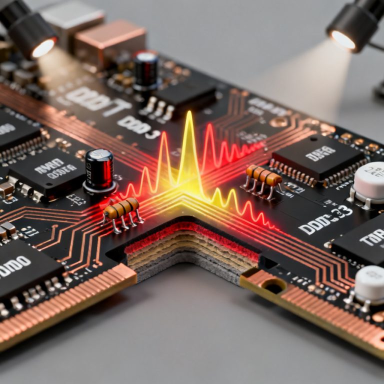
Why Copper Thickness High Speed PCB Matters
Copper thickness high speed PCB engineers specify is a fundamental design variable that affects every core performance metric of high-speed PCBs. Unlike low-frequency conventional circuit boards where copper selection only serves power conduction and heat dissipation, high-speed designs running Gigabit Ethernet, PCIe, USB4, DDR and RF signals require precise control over copper weight to maintain stable signal propagation. Proper return path design also depends on consistent copper thickness across reference planes.
The three core impacts of copper thickness high speed PCB include current carrying capability, controlled impedance stability, and high-frequency insertion loss. Additionally, copper specification directly decides fabrication difficulty, production tolerance, yield rate and overall PCB cost.
A widespread industry mistake is designing copper thickness high speed PCB solely for DC current demand. This narrow approach causes unexpected impedance drift, degraded eye diagrams, higher signal attenuation, crosstalk rise and intermittent system communication failures after mass production. In professional high-speed stackup design, copper thickness must be locked in the early stackup simulation stage, not adjusted randomly after layout completion. Understanding the physical and electrical rules of copper thickness high speed PCB allows designers to balance signal integrity, thermal performance, manufacturability and budget perfectly.
Standard Copper Thickness High Speed PCB Options (oz, μm, mil & Applications)
PCB manufacturers globally use ounce (oz per square foot) as the standard unit for copper weight, with unified conversion to micrometers and mils for stackup simulation and impedance calculation. Each copper thickness high speed PCB grade has fixed characteristics and targeted high-speed application scenarios.
| Copper Weight | Thickness (μm) | Thickness (mil) | Typical High-Speed PCB Application |
|---|---|---|---|
| 0.5 oz | 17.5 | 0.7 | Fine-line routing, high-density BGA, compact high-speed consumer boards, 10Gbps+ ultra-fine signal traces |
| 1 oz | 35 | 1.4 | Universal high-speed benchmark, 1–10Gbps digital signals, standard impedance-controlled traces, communication, industrial and server mainstream PCBs |
| 2 oz | 70 | 2.8 | High-current power layers, power supply bus traces, mixed-signal boards with both high-speed signals and high-power circuits |
| 3 oz & above | 105+ | 4.2+ | Heavy copper power modules, industrial control, automotive high-current boards, rarely used for pure high-speed signal layers |
0.5oz thin copper supports ultra-fine line etching, ideal for high-density routing where trace width and spacing are extremely limited. 1oz remains the industry default for high-speed signal layers due to its balanced performance in impedance control, low loss and manufacturing compatibility. When selecting copper thickness high speed PCB for your project, 1oz is the safest starting point for 1–10Gbps signals.
It is important to note that nominal copper thickness differs from finished copper thickness. Due to plating and etching loss, standard 1oz base copper usually ends up at 30–40μm on finished boards, with a typical industry tolerance of ±15%~20%.
How Copper Thickness High Speed PCB Affects PCB Controlled Impedance
Controlled impedance is the foundation of reliable high-speed signal transmission, required by nearly all modern high-speed protocols including PCIe, USB4, Ethernet and differential DDR interfaces. Copper thickness high speed PCB is a key input in microstrip and stripline impedance calculation formulas.
The core rule is clear: Copper thickness increases → characteristic impedance decreases. If designers upgrade copper from 1oz to 2oz without modifying trace width or dielectric thickness, trace impedance will drop by 5% to 8%. Most high-speed designs require impedance tolerance within ±5%; a deviation beyond this range triggers severe signal reflection, waveform distortion, closed eye diagrams and link connection failures. For a complete understanding of how copper thickness interacts with impedance formulas and tolerance grades, refer to Impedance Matching PCB.
To compensate impedance deviation caused by thicker copper, two practical methods are adopted in engineering: reduce trace width by 5%–8% to offset impedance drop, or increase dielectric thickness between signal trace and reference plane. For mass production stability, impedance simulation must fix copper thickness high speed PCB first in stackup design. Avoid adjusting trace width blindly after layout, as it will break routing density and spacing rules.
Copper Thickness High Speed PCB, Skin Effect and Insertion Loss
Insertion loss refers to signal attenuation during propagation along PCB traces, which limits maximum transmission speed and communication distance. Conductor loss and dielectric loss are the two main components of total insertion loss.
At low frequency and DC status, thicker copper reduces resistance and lowers conductor loss effectively. However, once the frequency rises above 3Gbps, the skin effect dominates signal behavior. High-frequency alternating current no longer flows evenly across the entire copper cross-section but concentrates only on the surface layer of the copper foil. As frequency increases, skin depth shrinks rapidly.
Under skin effect rules, increasing copper thickness high speed PCB beyond the skin depth brings almost no improvement in high-frequency loss. For 10Gbps+ ultra-high-speed channels, blindly choosing 2oz or thicker copper cannot reduce signal attenuation; it only raises cost and complicates impedance control. Designers must separate low-frequency power design from high-speed signal design: thick copper benefits power layers, while high-speed signal layers prioritize reasonable standard thickness and low-roughness copper material.
Copper Roughness: The Overlooked Factor for 3Gbps–10Gbps+ Designs
Most engineers focus only on copper thickness while ignoring copper foil roughness, which becomes the dominant factor of high-frequency loss above 3Gbps. Rough copper surfaces distort electromagnetic field distribution, extend the effective signal path and generate far more attenuation than minor copper thickness changes. For modern ultra-high-speed PCBs, roughness selection is more critical than copper weight tuning.
Three mainstream copper foil types are widely standardized for high-speed applications:
| Copper Foil Type | Roughness (Rz) | Suitable Bandwidth | Application Scenario |
|---|---|---|---|
| STD Standard Foil | >5μm | ≤3Gbps | General low-speed digital, cost-sensitive non-high-speed layers |
| RTF Reverse Treated Foil | 3–5μm | 3–10Gbps | Gigabit Ethernet, DDR4, mainstream mid-range high-speed interfaces |
| HVLP Ultra-Low Profile Foil | <2μm | 10Gbps+ | PCIe 4.0/5.0, USB4, 25G/100G Ethernet, server, AI and high-end communication hardware |
Standard STD copper is cost-effective but unsuitable for multi-Gbps designs due to high surface scattering loss. RTF foil balances cost and performance for most mainstream high-speed projects. HVLP ultra-low roughness copper is mandatory for 10Gbps+ channels, even when using standard copper thickness high speed PCB like 1oz. When routing high-speed signals on thin copper, following Differential Pair Routing Rules ensures proper length matching and impedance control.
Copper Thickness High Speed PCB vs Current Carrying Capacity (IPC Standard)
Copper thickness high speed PCB directly determines trace current carrying capacity, calculated based on IPC-2221 industry standards. Thicker copper provides larger cross-sectional area, supporting higher current under the same temperature rise condition. With a common 10°C temperature rise design threshold and 1mm trace width: 1oz copper carries approximately 1A, and 2oz copper carries approximately 2A.
Designers must clarify a clear boundary: high-speed signal traces only carry milliamp-level small current. They never require 2oz or heavy copper for current reasons. Only power planes, module power input traces and high-current bus lines need thick copper to avoid overheating, voltage drop and trace burnout. The best practice is adopting mixed copper thickness high speed PCB stackup: use 0.5oz/1oz for signal layers to guarantee signal integrity, and 2oz/3oz only for inner power layers to meet current and thermal demands.
PCB Manufacturing Capability, Process Limits and Cost Impact
Standard 0.5oz and 1oz copper fully match conventional PCB etching, lamination and plating processes, supporting fine line width, tight spacing and precise impedance control with stable yield. Copper thickness high speed PCB above 2oz requires specialized deep etching and heavy copper electroplating processes. Longer etching time increases risks of trace undercut, width deviation and out-of-tolerance impedance. Meanwhile, thick copper boards have higher risk of layer warpage and lamination deformation.
In terms of cost, copper weight is positively correlated with material and processing expenses. Upgrading from 1oz to 2oz usually increases PCB cost by 15%–25%, while 3oz and above heavy copper brings a cost premium of 80%–120% and longer lead time. Unnecessary thick copper selection wastes budget and introduces hidden signal integrity risks. Designers should confirm manufacturer process capability and cost budget before finalizing copper thickness high speed PCB specifications.
Common Copper Thickness High Speed PCB Myths in High-Speed Design
Myth: 1oz copper is exactly 35μm.
Fact: Finished 1oz copper ranges from 30–40μm due to plating and etching loss with ±15% typical tolerance.
Myth: Thicker copper always reduces high-speed insertion loss.
Fact: Above 3Gbps, skin effect takes over; roughness matters more than thickness.
Myth: All layers should use the same copper thickness high speed PCB.
Fact: Mixed copper stackup optimizes signal performance, current capacity and cost simultaneously.
Myth: Current demand alone decides copper thickness.
Fact: High-speed signals prioritize impedance and loss instead of current carrying capability.
Key Takeaways & Design Best Practices
- 1oz copper is the universal benchmark for most 1–10Gbps high-speed signal layers with the best balance of performance, manufacturability and cost.
- Reserve 2oz and heavier copper only for power layers; avoid thick copper on high-speed signal traces to prevent impedance deviation.
- For 10Gbps+ ultra-high-speed designs, prioritize HVLP low-roughness copper over blindly increasing copper thickness.
- Use 0.5oz thin copper for high-density BGA and fine-line routing to save layout space while maintaining impedance control.
- Adopt mixed copper thickness stackup to separate signal layer and power layer specifications.
- Lock copper thickness high speed PCB in early stackup simulation to avoid later rework and manufacturing deviation.
- Always refer to IPC-2221 and IPC-6012 standards for current capacity and finished copper tolerance.
For a complete understanding of impedance formulas and tolerance grades that work together with copper thickness, refer to the impedance control guide.
FAQ About Copper Thickness High Speed PCB
What is the most common copper thickness for high-speed PCB?
1oz (35μm / 1.4mil) is the standard choice for almost all mainstream high-speed signal layers.
Will 2oz copper affect 50Ω impedance?
Yes. Switching from 1oz to 2oz reduces impedance by 5%–8%; you need to reduce trace width accordingly for compensation.
Is thicker copper better for high-frequency signal loss?
No. Above 3Gbps, skin effect limits effective conduction; copper roughness impacts loss far more than thickness.
When should I use HVLP ultra-low profile copper?
Mandatory for 10Gbps+ interfaces such as PCIe 4.0/5.0, USB4 and 100G Ethernet.
Does heavy copper PCB cost much more?
Yes. 2oz costs 15%–25% more than 1oz; 3oz+ heavy copper can raise cost by over 80%.
Get Custom Copper Thickness High Speed PCB Stackup Recommendation
Choosing the right copper thickness high speed PCB requires professional signal integrity simulation and manufacturing experience. Every project has unique requirements in data rate, layer count, trace density, current load and cost budget. If you need professional copper thickness selection, impedance tuning, high-speed stackup design or PCB manufacturing quotation, our engineering team can provide fully customized design suggestions matched with your application scenario.
Send us your board specification, signal rate and current demand, and we will deliver optimized copper thickness high speed PCB solutions and free project evaluation.
© 2026 HighSpeedPCBs