Power integrity high speed PCB design is the foundation of stable, noise-free power delivery for FPGAs, CPUs, and memory chips. This comprehensive guide covers PDN target impedance, decoupling capacitor placement, ground bounce noise suppression, and PI simulation for reliable signal integrity.
This power integrity high speed PCB guide is part of our Signal Integrity Guide.
Table of Contents
- 1. What is Power Integrity (PI) in High-Speed PCB?
- 2. Power Integrity is the Foundation of Signal Integrity
- 3. PDN Target Impedance Design Method
- 4. Decoupling Capacitor Selection and Placement
- 5. Ground Bounce and Simultaneous Switching Noise
- 6. Power Plane Design for Low Noise
- 7. PI Simulation and Measurement
- 8. Common PI Problems and Fixes
- 9. Key Takeaways
- 10. FAQ
- 11. Need PDN Optimization?
What is Power Integrity (PI) in High-Speed PCB?
Power integrity high speed PCB refers to the capability of a printed circuit board to deliver stable, clean, and noise-free power supply voltage to integrated circuits, FPGAs, CPUs, memory chips and other high-speed loads throughout all operating conditions. It covers the full design scope including Power Distribution Network (PDN) impedance control, power supply ripple suppression, decoupling network deployment, and mitigation of ground bounce noise and simultaneous switching noise.
With the continuous evolution of high-speed digital systems, semiconductor chips are trending toward lower supply voltage, larger transient current, and tighter voltage margin tolerance. Traditional PCB power design methods can no longer meet the demands of high-speed signal transmission. Uncontrolled power noise and excessive PDN impedance will directly degrade system stability, trigger transmission errors, and even cause intermittent system crashes. For high-speed PCB design, power integrity high speed PCB has become an indispensable core discipline alongside signal integrity.
Power Integrity is the Foundation of Signal Integrity
2.1 How Power Noise Degrades Signal Performance
Power integrity high speed PCB and signal integrity (SI) are tightly coupled in high-speed PCB design, and poor PI performance is the root cause of most signal integrity failures. Power supply noise distorts signal transmission through multiple physical mechanisms: unstable reference voltage induces jitter at signal receiving ends, leading to incorrect logic level judgment and increased bit error rate. Power ripple modulates clock signals and generates significant clock jitter, narrowing the eye diagram opening and reducing noise margin. Meanwhile, Simultaneous Switching Noise (SSN) triggers severe ground bounce noise, causing signal amplitude collapse, waveform distortion and false triggering of digital circuits.
For a deeper understanding of how power noise affects eye diagram quality, see our Eye Diagram and Jitter Analysis Guide.
2.2 Correlation Between PI and SI Issues
| Problem Type | Manifestation of PI Impact on SI |
|---|---|
| Excessively high PDN impedance | Insufficient chip power supply and weakened driving capability |
| Large power supply ripple | Blurred eye diagram and reduced noise immunity |
| Ground bounce noise | Compressed signal amplitude and erroneous logic level identification |
| Resonance spike | Excessive EMI at specific frequencies and aggravated clock jitter |
Without a well-optimized power integrity high speed PCB design, even perfect signal routing, controlled impedance and length matching cannot guarantee reliable high-speed signal transmission. PI lays the physical foundation for stable SI performance.
For guidance on impedance control that affects PDN performance, see our Impedance Matching Ultimate Guide.
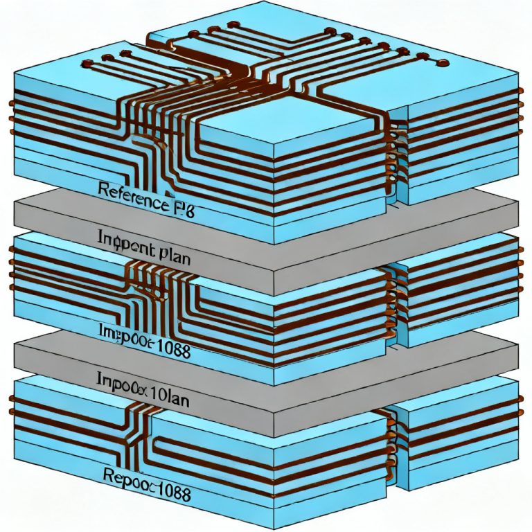
PDN Target Impedance Design Method
3.1 What is PDN?
The Power Distribution Network (PDN) represents the entire power delivery path on a high-speed PCB, ranging from the Voltage Regulator Module (VRM), power traces, power/ground planes, decoupling capacitors, packaging pins, all the way to the power supply pins of the load chip. The core goal of PDN design PCB is to maintain the system impedance below a predefined target value across the full operating frequency range, ensuring voltage fluctuation stays within the allowable ripple specification under transient current changes.
3.2 Target Impedance Formula
The industry-standard formula for calculating PDN target impedance is defined as:
Z_target (Ω) = VDD × Ripple% / ΔI
Where VDD is the nominal supply voltage of the chip, Ripple% is the allowable power supply voltage ripple percentage, and ΔI stands for the maximum transient current variation of the load. This formula quantifies the upper impedance limit that the PDN must maintain to suppress voltage drop and ripple.
3.3 Standard PDN Design Workflow
| Step | Content | Description |
|---|---|---|
| 1 | Confirm chip current demand | Obtain static and transient current parameters from component datasheets |
| 2 | Calculate target impedance | Typical range controlled within 10–100 mΩ for most high-speed devices |
| 3 | Build PDN model | Integrate VRM model, decoupling capacitor parameters, and PCB parasitics |
| 4 | Simulate PDN impedance | Analyze impedance-frequency curve to check resonance |
| 5 | Optimize capacitor combination | Match multi-value capacitors to flatten impedance peaks |
3.4 Typical Target Impedance Reference for Common Chips
| Chip Type | Typical Z_target Range |
|---|---|
| General IO Interface Chip | 100–200 mΩ |
| DDR Memory Series | 30–50 mΩ |
| FPGA / ASIC Core | 10–30 mΩ |
| CPU / AI High-Speed Computing Chip | 1–10 mΩ |
Decoupling Capacitor Selection and Placement
4.1 Multi-Range Capacitor Combination Principle
Decoupling capacitors are the most critical component for PDN impedance optimization and noise suppression in power integrity high speed PCB design. A hierarchical combination of different capacitance values is required to cover DC to GHz full frequency bands.
Capacitor TypeCapacitance RangeEffective FrequencyCore ApplicationBulk Large-Capacity10µF – 1000µFDC – 1MHzLow-frequency decoupling and energy storageMLCC Ceramic0.1µF – 10µF1MHz – 100MHzMid-frequency decoupling, main band noise suppressionHigh-Frequency Small100pF – 1nF100MHz – 1GHzSuppress high-frequency switching spikes
4.2 Golden Rules for Capacitor Layout
Reasonable decoupling capacitor placement is as important as capacitor selection, directly determining parasitic inductance and decoupling effectiveness.
| Rule | Core Target | Key Design Points |
|---|---|---|
| Minimize loop inductance | Reduce parasitic inductance | Place capacitors as close as possible to chip power/ground pins |
| Shorten via and routing | Suppress high-frequency impedance | Connect capacitor pads directly to planes with shortest vias |
| Multi-stage matching | Full-frequency noise suppression | Combine large, medium and small capacitance in parallel |
| Uniform distributed layout | Avoid planar resonance | One decoupling capacitor per 4–6 power pins in BGA areas |
For via design considerations affecting decoupling effectiveness, see our Return Path Design Guide.
Ground Bounce and Simultaneous Switching Noise
5.1 Origin of Simultaneous Switching Noise
Simultaneous Switching Noise (SSN) is one of the primary causes of ground bounce noise in high-speed PCB design. When multiple IO pins of a chip switch logic levels simultaneously, instantaneous large current flows through chip packaging inductance, PCB trace inductance and ground loop path. According to the electromagnetic induction principle, voltage bounce is generated on the ground and power loops.
The theoretical calculation formula for ground bounce noise voltage is:
V_bounce = L_total × di/dt
L_total refers to the total parasitic inductance of the power-ground loop, while di/dt represents the rate of instantaneous current change during signal switching. The faster the switching speed and the more pins flipping simultaneously, the more severe the ground bounce noise.
5.2 Impacts and Improvement Countermeasures
| Countermeasure | Functional Effect |
|---|---|
| Increase ground pins and complete ground planes | Reduce power-ground loop parasitic inductance |
| Limit simultaneous switching IO pins | Lower di/dt value and suppress noise excitation |
| Deploy sufficient nearby decoupling capacitors | Provide local charge compensation for transient current |
| Adjust driver strength and slew rate control | Prolong switching time and reduce current change rate |
For crosstalk issues that may compound with switching noise, see our Crosstalk Guide.
Power Plane Design for Low Noise
6.1 Tight Coupling of Power and Ground Planes
Power and ground plane stacking is the foundation of low-impedance PDN design. Adopting thin dielectric substrates with 2–4mil thickness between power and ground layers realizes tight planar coupling. This structure forms embedded natural capacitance between power and ground planes, reaching 30–50pF per square inch, providing inherent high-frequency decoupling capability without additional capacitors. Tight coupling also effectively reduces planar parasitic inductance, flattening PDN impedance curve in mid and high frequency bands.
6.2 Planar Resonance Phenomenon and Suppression
| Phenomenon | Root Cause | Suppression Methods |
|---|---|---|
| Uneven power voltage distribution | Irregular plane shape and split slots | Add stitching vias to optimize planar integrity |
| PDN impedance spike at specific frequency | Natural resonance between power and ground planes | Deploy shunt damping capacitors and increase planar loss |
6.3 Integrity of Reference Planes
A continuous and complete ground plane is the basic guarantee of power integrity high speed PCB and signal return path integrity. Any arbitrary plane splitting, slot crossing and routing across power/ground gaps will destroy the integrity of PDN and signal return path, causing increased impedance, resonance noise and crosstalk. High-speed signal traces must avoid crossing split reference planes in PI and SI co-design.
For detailed guidance on reference plane continuity, see our Return Path Design Guide.
PI Simulation and Measurement
7.1 Mainstream Power Integrity Simulation Types
Modern high-speed PCB PI design relies heavily on simulation to avoid trial-and-error costs. Frequency-domain simulation focuses on PDN impedance curve analysis, ensuring full-frequency impedance is lower than the calculated target impedance. Time-domain simulation analyzes voltage drop, transient ripple and ground bounce noise under actual chip working current excitation.
Widely used professional PI simulation tools include Sigrity PowerSI, Ansys SIwave and Keysight ADS PIPro, which support full-stack PCB PDN modeling, resonance analysis and capacitor optimization iteration.
7.2 Practical PI Measurement Methods
| Test Instrument | Main Application |
|---|---|
| Oscilloscope + Power Probe | Measure time-domain power ripple, voltage drop and ground bounce |
| Vector Network Analyzer (VNA) | Test PDN S-parameters and extract actual impedance |
| Spectrum Analyzer | Detect conducted EMI noise on power lines and locate resonance |
Common PI Problems and Fixes
| Common Problem | Possible Root Cause | Targeted Solutions |
|---|---|---|
| Power ripple exceeds 5% specification | Insufficient decoupling capacitors | Add bulk and MLCC mid-frequency capacitors |
| Resonance spike at tens of MHz | Power-ground plane resonance | Add parallel damping resistors to suppress resonance |
| High-frequency noise glitches | Insufficient high-frequency decoupling | Deploy 100pF–1nF small capacitors close to chip pins |
| Instantaneous voltage drop | Slow response of distant capacitors | Arrange high-value bulk capacitors closer to load chip |
| PDN simulation impedance over limit | Unreasonable capacitor combination | Optimize multi-stage capacitance and follow placement rules |
Key Takeaways for Power Integrity High Speed PCB
- Power integrity high speed PCB is the cornerstone of signal integrity, and the two must be designed collaboratively
- Adopting the PDN target impedance design method quantifies and optimizes power delivery performance
- Decoupling capacitors must follow the large-medium-small multi-stage combination strategy
- Tightly coupled power-ground plane stacking naturally reduces PDN impedance
- Early PI simulation eliminates resonance, voltage drop and noise problems before board production
- Proper decoupling capacitor placement and ground bounce noise suppression are critical for high-speed reliability
Return to the Signal Integrity Guide for more coverage of impedance control, return path design, differential pairs, crosstalk, eye diagram, reflection termination, and power integrity.
Frequently Asked Questions About Power Integrity for High-Speed PCB
Q1: What is the target impedance in PDN design for power integrity high speed PCB?
Target impedance is the maximum allowable PDN impedance calculated by Z_target = VDD × Ripple% / ΔI. Keeping PDN impedance below this value ensures stable power delivery under transient current changes. This is a core concept in power integrity high speed PCB design.
Q2: How to select decoupling capacitors for power integrity high speed PCB?
Use a multi-stage combination: bulk capacitors (10µF–1000µF) for low frequency, MLCCs (0.1µF–10µF) for mid frequency, and small capacitors (100pF–1nF) for high frequency. Proper decoupling capacitor placement is equally important as selection for power integrity high speed PCB.
Q3: What causes ground bounce noise in high-speed PCB?
Ground bounce noise is caused by simultaneous switching noise (SSN) when multiple IO pins switch simultaneously. The voltage bounce follows V_bounce = L_total × di/dt. Higher switching speed and more parallel pins increase ground bounce noise.
Q4: How does power integrity affect signal integrity?
Poor PI causes excessive PDN impedance (weak driving), power ripple (blurred eye diagram), ground bounce noise (compressed amplitude), and resonance spikes (EMI/clock jitter). Power integrity high speed PCB is the foundation of stable signal transmission.
Q5: What PI simulation tools are recommended for power integrity high speed PCB?
Sigrity PowerSI, Ansys SIwave, and Keysight ADS PIPro are industry standards for PDN impedance analysis, resonance checking, and capacitor optimization in power integrity high speed PCB design.
Need PDN Optimization for Your High-Speed PCB Project?
If you are undertaking high-speed PCB design for FPGA, CPU, AI chips or DDR memory systems and encounter PDN impedance overshoot, power ripple, ground bounce noise or EMI issues, our professional team provides free decoupling capacitor scheme customization and free PDN simulation consulting services.
We offer: Free power integrity high speed PCB consultation • Decoupling capacitor selection and placement optimization • PDN simulation and resonance analysis • Power plane stacking design guidance
All design files strictly confidential. Response within one business day.
About HighSpeedPCBs.com
We are a specialized PCB design and manufacturing service provider serving industrial, automotive, medical, and communications OEMs worldwide. Our expertise in power integrity high speed PCB design ensures your high-speed interfaces perform reliably with stable power delivery.
© 2026 HighSpeedPCBs.com — Professional High-Speed PCB Solutions