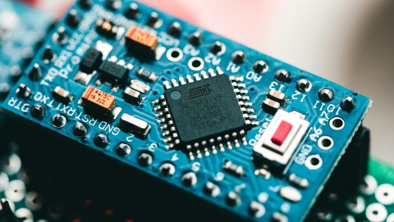
High-speed PCB prototyping and mass production services are the core of modern high-frequency electronics. We are a direct factory manufacturer with over 10 years of experience, providing reliable, cost-effective solutions for your projects.As a direct factory manufacturer with over 10 years of specialized experience in customized high-speed PCB production, we deliver one-stop solutions: high-speed PCB prototyping, fast-turn urgent PCB production, low-volume trial production, medium & large-batch manufacturing, HDI high-density interconnection, high-frequency substrate PCB fabrication, and optional full PCBA assembly services.
We support 24/48/72-hour expedited prototyping, precision impedance control, back drilling, buried & blind vias, resin plug holes, and ultra-fine circuit processing. Fully compliant with global IPC standards and international certifications, our in-house engineering team provides free DFM review, stackup design, and professional impedance calculation. We supply stable, cost-effective customized high-speed PCBs for hardware engineers, procurement managers, startup teams, and enterprise NPI projects. Every order is delivered with complete test reports, full batch traceability, and worldwide DDP door-to-door shipping.
1. Your Trusted High-Speed PCB Manufacturing Partner
In the modern high-speed electronics industry, signal integrity, low signal loss, stable impedance performance, and structural reliability directly determine the service life and working efficiency of high-end electronic devices. Conventional standard FR4 circuit boards cannot meet strict requirements for high-speed data transmission, high-frequency operation, and high-density miniaturized wiring. For advanced R&D and commercial mass production, professional custom high-speed PCB manufacturing is no longer optional — it is essential.
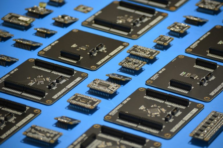
We are a manufacturer focused exclusively on high-speed PCBs, not a general-purpose circuit board factory. We specialize in high-speed, high-frequency, multi-layer, and high-precision PCB fabrication. Our service coverage includes fast-turn PCB prototype online services, small-batch functional verification, and large-scale stable mass production.
Equipped with self-owned production facilities, imported precision production & testing equipment, and an experienced engineering team familiar with international IPC standards, we eliminate middleman markups and offer direct factory pricing. We balance premium quality, flexible lead times, and competitive costs to serve global B2B buyers.
1.1 Who We Serve
We support the complete life cycle of electronic product development and meet diversified global customer demands:
| Customer Type | Core Challenges | How We Support You |
|---|---|---|
| Hardware Engineers | Rapid design validation & accurate performance testing | 24–72h fast high-speed PCB prototype + official TDR impedance reports |
| Procurement Managers | Stable supply, cost control & low supply chain risks | Long-lead material stocking, VMI inventory management & consistent batch quality |
| Startup Teams | Low-budget iteration, small orders & fast time-to-market | Low MOQ, free DFM inspection & cost-effective prototyping |
| Large Enterprises | NPI integration, complex high-speed processes & long-term mass supply | Custom HDI, back drilling, via-in-pad & any-layer HDI solutions |
1.2 Our Core Services
- Fast-turn prototyping: 24h/48h/72h urgent delivery for time-critical projects
- Small-batch production: 5–100 units for functional testing and market trial sales
- Mass manufacturing: 100 to 100,000+ units for long-term global continuous supply
- One-stop PCBA service: Component sourcing, SMT mounting, wave soldering and finished product testing
1.3 Why Choose Our High-Speed PCB Services
- 10+ years of concentrated expertise in high-speed & high-frequency PCB manufacturing
- In-house factory with full independent control over production, inspection and quality management
- Free DFM review, stackup optimization and precise impedance calculation for all inquiries
- Mature high-speed process portfolio: precision impedance control, back drilling, HDI & any-layer interconnection
- Multilingual engineering support and flexible global logistics solutions
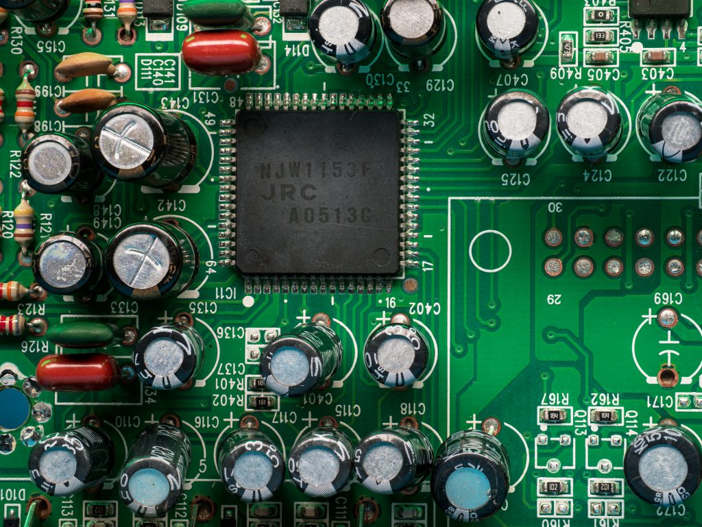
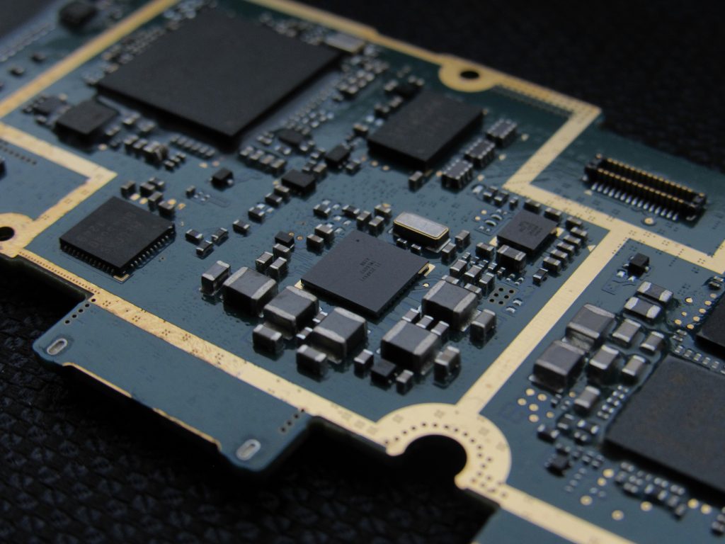
2. Core High-Speed PCB Manufacturing Capabilities
Clear manufacturing capability specifications help engineers and global buyers quickly evaluate project feasibility. Below are standardized general specifications, exclusive high-speed processes, premium substrate options, surface treatment solutions, and professional testing capabilities — with full transparency for both standard and advanced customized options.
2.1 General PCB Fabrication Specifications
| Parameter | Standard Capability | Advanced Custom Capability |
|---|---|---|
| Layer Count | 2–32 Layers | Custom 34+ Layers |
| Board Thickness | 0.4mm – 3.2mm | Custom thickness over 3.2mm |
| Maximum Panel Size | 500mm × 600mm | Non-standard customized dimensions |
| Minimum Line Width / Spacing | 4/4 mil (0.1mm) | 3/3 mil / 2/2 mil ultra-fine traces |
| Minimum Drill Hole | 0.2mm Mechanical Drilling | 0.1mm laser microvia drilling |
| Aspect Ratio | 10:1 | 15:1 high aspect ratio processing |
| Copper Thickness | 0.5oz – 5oz | Custom 6oz+ heavy copper |
What is Aspect Ratio?
Aspect ratio refers to board thickness divided by the minimum drill hole diameter. The standard 10:1 ratio suits most commercial high-speed PCB designs. For high-demand 15:1 projects, we adopt specialized electroplating and drilling technology to ensure structural stability with a reasonable cost increase.
2.2 Exclusive High-Speed Process Capabilities
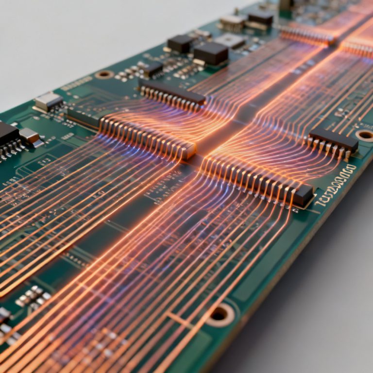
High-speed circuits require strict control over signal attenuation, resonance interference and structural precision. Our dedicated high-speed manufacturing processes ensure stable transmission performance for 10Gbps, 25Gbps, 50Gbps and next-generation high-rate applications.
| High-Speed Process | Standard Specification | Custom Solution for Strict Applications |
|---|---|---|
| Impedance Tolerance | ±10% General Grade | ±7% precision control / ±5% ultra-precision (engineering evaluation required) |
| Back-Drilling Tolerance | ±0.05mm | Remove redundant via stubs to reduce signal reflection and loss |
| Back-Drilling Range | 1–6 Layers | Custom deep multi-layer back drilling |
| Buried & Blind Via | 1+N+1 / 2+N+2 HDI | Any-layer HDI for servers & high-density computing hardware |
| Resin Plug Hole | Flattened copper surface | Meet via-in-pad requirements for compact BGA layouts |
2.3 Impedance Tolerance Selection Guide
| Tolerance Grade | Typical Applications | Cost Impact |
|---|---|---|
| ±10% | PCIe Gen3/4, USB 3.0, Gigabit Ethernet | Standard, fully included |
| ±7% | DDR4/DDR5, 10G–25G serial links, RF circuits | Minor additional cost |
| ±5% | High-sensitivity RF, microwave, 50G+ high-speed links | Custom engineering assessment required |
2.4 High-Speed & High-Frequency Material Selection
Base materials directly affect Dk/Df parameters, high-frequency loss, and long-term operational stability. We cooperate with world-renowned high-speed substrate brands to provide multi-grade material options for different loss budgets and application scenarios:
| Brand | Material Series | Loss Level | Recommended Application |
|---|---|---|---|
| Rogers | RO3000, RO4000, RO5880 | Low to Ultra-Low | RF, microwave & 5G communication modules |
| Panasonic | Megtron 4 / 6 / 8 | Low to Ultra-Low | AI servers & high-speed computing equipment |
| Isola | FR408, I-Speed, Tachyon | Medium to Ultra-Low | High-reliability industrial control systems |
| Taconic | RF Series | Low Loss | Professional high-frequency wireless devices |
| Shengyi | S7000 / S9000 | Medium to Low | Cost-effective mainstream high-speed PCBs |
| Standard FR4 | TG130 / TG170 | Standard Loss | General commercial high-speed circuits |
2.5 Multiple Surface Finish Options
Each surface finish offers unique advantages in oxidation resistance, solderability, high-frequency loss and cost, helping you select the most suitable solution:
| Surface Finish | Best Application | Core Advantage | Cost Level |
|---|---|---|---|
| ENIG (Immersion Gold) | BGA & fine-pitch components | Ultra-flat surface, anti-oxidation & stable soldering | Medium |
| ENEPIG | Gold fingers & wire bonding | Custom thick gold plating available | High |
| OSP | Fast prototyping & cost-sensitive orders | Lowest cost & eco-friendly | Low |
| Immersion Silver | High-frequency high-speed circuits | Minimal high-frequency signal loss | Medium |
| Hard Gold Plating | Repeatedly plugged gold fingers | Excellent wear resistance | High |
3. Professional High-Speed PCB Prototyping Services
R&D iteration, design validation and hardware debugging rely on reliable, high-quality high-speed PCB prototype manufacturing. We operate independent prototyping production lines and streamlined approval workflows to resolve common pain points of long lead times and high costs from traditional high-speed PCB factories.
Whether you need multi-layer complex boards, HDI structures, Rogers high-frequency materials or fully impedance-controlled designs, we deliver accurate prototypes with complete technical documents.
3.1 Flexible Prototyping Options
| Service Type | Quantity | Lead Time | Ideal Application |
|---|---|---|---|
| Standard Prototyping | 1–10 pcs | 5–7 Working Days | Conventional functional verification |
| 48h Expedited Service | 1–5 pcs | 48 Hours | Urgent project modification & demo samples |
| 72h Expedited Service | 1–5 pcs | 72 Hours | 4–8 layer medium-complexity high-speed PCBs |
| Rapid Iteration | 5–20 pcs | 3–5 Working Days | Multi-round design optimization & comparison testing |
3.2 Complete Deliverables for Every Prototype
- Official TDR impedance test report for critical high-speed signal lines
- Complete flying probe electrical test report to eliminate open/short defects
- Custom micro-section photos (on request) for lamination & hole structure inspection
- Pre-production Gerber file confirmation to ensure 100% design consistency
3.3 Standard Prototyping Workflow
Step 1: Submit Gerber Files
→ Step 2: Engineering DFM Review (Reply within 24 hours)
→ Step 3: Official Quotation (4–8 hours)
→ Step 4: Priority Production Scheduling
→ Step 5: Professional Testing + Report Delivery + Global Shipping
3.4 Free DFM Design Inspection
Every prototype order includes a comprehensive free DFM pre-review. Our engineers strictly inspect key production indicators:
| DFM Inspection Item | Production Standard |
|---|---|
| Minimum Line Width / Spacing | 4/4 mil standard, 3/3 mil advanced support |
| Outer Layer Annular Ring | ≥0.1mm |
| BGA Fanout Design | Via-in-pad matched with resin plug technology |
| Solder Mask Dam Width | ≥3 mil between dense BGA pads |
| Board Aspect Ratio | ≤10:1 standard, 15:1 custom |
| Layer Stack Symmetry | Symmetric structure to prevent board warpage |
We provide reasonable design optimization suggestions without changing your original design logic, effectively improving production yield and avoiding rework.
4. Scalable Mass Production & Low Volume PCB Assembly Solutions
After prototype verification and design finalization, stable and consistent mass production determines successful product commercialization. We realize seamless transition from high-speed PCB prototype to large-scale manufacturing with unified material standards, process parameters and quality control specifications.
4.1 Mass Production Tiers
| Production Tier | Quantity Range | Application Scenario |
|---|---|---|
| Small-Batch Production | 10–100 pcs | Trial production validation & small-scale equipment supporting |
| Medium-Batch Production | 100–1,000 pcs | Official product launch & regional market promotion |
| Large-Volume Production | 1,000–100,000+ pcs | Long-term framework cooperation & global bulk supply |
4.2 Stable Mass Production Support
- Fixed production processes and raw material standards to ensure consistent batch-to-batch quality
- Stocking solutions for long-lead imported high-frequency materials to avoid delivery delays
- VMI vendor managed inventory service to reduce customer inventory pressure and capital occupation
4.3 NPI New Product Introduction Support
Our engineering team provides full NPI services, including process difficulty assessment, high-speed stackup optimization, and pilot run parameter adjustment, ensuring a smooth transition from R&D trial production to stable mass output.
4.4 Low Volume PCB Assembly Service
To meet one-stop procurement demands, we provide flexible low volume PCB assembly services, including component sourcing, SMT mounting, wave soldering, functional testing and finished product packaging. One-stop cooperation covers PCB manufacturing and board-level assembly to simplify your supply chain.
5. Full-Cycle Engineering & Technical Support
High-speed PCB design involves complex technical details, including layer stack structure, differential impedance matching, high-frequency material loss parameters and high-density via optimization. Our professional engineering team provides free full-cycle technical support to resolve design and production challenges.
5.1 Custom Stackup Design Support
Based on your layer count, board thickness, target impedance and operating frequency, we offer free customized high-speed stackup suggestions. Complete stackup documents can be directly imported into Altium Designer, Cadence, KiCad and other mainstream design software.
5.2 In-Depth DFM Review
Focused on high-speed manufacturing characteristics, we conduct in-depth document inspection for wiring rationality, process feasibility and high-speed compatibility. All potential production risks are highlighted in advance with clear, actionable improvement solutions.
5.3 Accurate Impedance Calculation
Different from ordinary theoretical calculators, we adopt actual production Dk/Df data from authorized material suppliers for impedance simulation and trace width calculation. Calculation results highly match mass production data, minimizing deviations between design targets and actual tested impedance values.
6. Testing & Verification — How We Guarantee Quality
Many PCB suppliers only calculate impedance on paper without real batch testing. We complete both theoretical calculation and physical verification for every high-speed PCB order.
6.1 Why Actual Testing Matters
Base materials have natural tolerance ranges. Dielectric thickness, etching depth and lamination conditions vary slightly in each production batch. Even precise stackup calculations cannot guarantee on-board impedance performance without physical testing. Batch verification is the core guarantee of signal integrity.
6.2 What Is an Impedance Coupon?
An impedance coupon is a dedicated test structure produced together with your PCBs. It undergoes the exact same lamination, etching and drilling processes. We test coupons instead of cutting finished boards to ensure accurate data without damaging your products.
6.3 TDR (Time Domain Reflectometry) Testing
TDR is the global industry standard for high-speed impedance measurement. It transmits high-speed pulse signals along transmission lines and captures reflection data to detect impedance fluctuations and discontinuities.
TDR test reports include:
- Actual measured impedance values for single-ended and differential lines
- Accurate positioning of impedance mutation points
- Clear pass/fail results based on your customized tolerance
6.4 Complete Testing Capabilities
| Test Type | Testing Scope | Application |
|---|---|---|
| TDR Impedance Test | Single-ended & differential impedance | All high-speed PCB batches |
| Flying Probe Test | Circuit continuity, open & short circuit | Prototypes & small batches |
| Fixture Functional Test | Mass electrical performance screening | High-volume production |
| X-Ray Inspection | BGA internal solder joints & buried via quality | HDI & high-density designs |
| Microsection Analysis | Hole copper thickness & lamination alignment | Process validation & quality audit |
| Thermal Cycling Test | Environmental reliability stability | Custom high-reliability projects |
6.5 Standard Included Deliverables
✅ Official TDR impedance test report
✅ Flying probe electrical test report
✅ Custom micro-section photos (on request)
✅ Pre-production Gerber confirmation document
7. Strict Quality Assurance & Industry Certifications
Stable quality and internationally recognized certifications are the foundation of long-term overseas B2B cooperation. All our high-speed PCBs are manufactured in strict accordance with global IPC industrial standards.
7.1 Authorized Global Certifications
| Certification | Qualification Status |
|---|---|
| ISO 9001:2025 | Fully certified & valid |
| UL 94V-0 | Fire resistance certified |
| RoHS / REACH | Full environmental compliance |
| IATF 16949 | Automotive-grade quality system available |
7.2 Full-Process Quality Control
| Quality Control Stage | Core Inspection Items |
|---|---|
| IQC Incoming Inspection | High-frequency substrates, copper foil & chemical raw materials |
| IPQC In-Process Control | Lamination, drilling, electroplating & surface treatment |
| FQC Final Quality Inspection | Appearance, dimensions, electrical performance & data audit |
7.3 Full Batch Traceability
Every order is assigned an independent production batch number. We permanently archive design files, process records, test reports and raw material batch information. If any after-sales issue occurs, we can quickly locate the root cause and provide targeted solutions.
8. Transparent Lead Time & Global Delivery Solutions
We formulate standardized lead times based on PCB layer count, process difficulty and production scale, and support diversified international logistics to ensure on-time global delivery.
8.1 Standard Working Day Lead Time
| Board Type | Prototyping | Small Batch <100pcs | Mass Batch 100–1000pcs |
|---|---|---|---|
| 4–6 Layer High-Speed PCB | 5–6 Days | 7–9 Days | 10–12 Days |
| 8–10 Layer High-Speed PCB | 6–8 Days | 9–11 Days | 12–15 Days |
| 12+ Layer Multi-Layer PCB | 8–10 Days | 12–14 Days | 15–18 Days |
| HDI / High-Frequency PCB | +2–4 Days | +3–5 Days | +5–7 Days |
Note: 24/48/72-hour ultra-expedited service is available for 4–8 layer urgent high-speed PCB prototype projects.
8.2 Global Shipping Options
| Shipping Method | Transit Time | Suitable Order Type |
|---|---|---|
| DHL / FedEx / UPS Express | 3–5 Working Days | Prototypes & small batches |
| Air Freight | 5–7 Working Days | Medium-batch urgent orders |
| Sea Freight | 20–30 Days | Large-volume cost-sensitive orders |
We provide professional DDP delivered duty paid services, covering customs declaration, tax payment and door-to-door delivery to simplify overseas procurement.
9. Typical Applications & Industry Expertise
We have rich manufacturing experience in high-speed PCBs for high-demand industrial and commercial scenarios:
| Application Field | Board Features | Core Technical Requirements |
|---|---|---|
| AI Servers & Accelerators | 12–16 layers, Megtron 6/8 material | ±7% impedance control, back drilling & HDI |
| 400G / 800G Optical Modules | Rogers RO4000 series | Ultra-low loss & high-frequency stability |
| 5G Base Station Hardware | Mixed FR4 + high-frequency dielectric | High temperature resistance & long-term signal stability |
| Industrial High-Speed Control | 8–10 layers, high-TG FR4 | Cost-effective mass production & high yield |
Anonymized industry case studies and factory equipment lists are available for qualified buyers upon request.
10. Simplified Quotation Process & Required Documents
We simplify the inquiry and quotation process with fully transparent pricing and no hidden fees, helping you quickly confirm project budgets.
10.1 Required Information for Quotation
| Required Item | Mandatory | Remarks |
|---|---|---|
| Gerber Files (.zip / RS-274X) | ✅ | Include drill, solder mask & silkscreen layers |
| Total Layer Count | ✅ | 2–32 layers standard, 34+ layers custom |
| Board Thickness & Copper Thickness | ✅ | Specify separate inner/outer copper thickness if needed |
| Impedance Specifications | ⚙️ | Target value + tolerance grade |
| PCB Material | ✅ | FR4, Rogers, Panasonic or manufacturer recommendation |
| Quantity & Required Lead Time | ✅ | Standard or expedited |
10.2 Efficient Quotation Process
- Submit design files and project requirements online instantly
- Professional high-speed PCB engineers complete file analysis within 2–4 hours
- Detailed official quotation issued within 4–8 working hours
- Production scheduled on the same day after customer confirmation
10.3 Free DFM Review with Every Quotation
Every inquiry includes a free professional DFM assessment. While providing quotations, our team marks potential production risks and offers practical optimization suggestions — no purchase obligation required.
11. High-Speed PCB Frequently Asked Questions
- What is your MOQ?1 piece for high-speed PCB prototype; 100 pieces for mass production.
- Do you support expedited production for 4–10 layer high-speed PCBs?Yes. 48-hour fast delivery is available for boards up to 8 layers. Custom urgent lead time is optional for 12+ layer projects.
- Will you provide official impedance test reports?Yes. Complete official TDR impedance test reports are provided for all impedance-controlled high-speed PCB orders.
- What is an impedance coupon?An impedance coupon is a dedicated test panel produced together with your PCBs. It is used for accurate impedance testing without damaging finished products.
- Do you have manufacturing experience for AI server and optical module PCBs?Yes. We have mature experience in 400G/800G optical modules, AI accelerator cards and data center multi-layer high-speed PCBs.
- Is there any tooling or NRE charge?A small NRE fee applies for individual prototype orders. Mass production orders enjoy free setup fees.
- Can you provide one-stop PCBA turnkey service?Yes. We offer full service including component sourcing, SMT assembly, soldering and functional testing.
- I only have PDF drawings and no Gerber files, what should I do?We provide professional PDF-to-Gerber conversion service with a low service fee.
- Do you offer DDP door-to-door delivery?Yes. DDP delivered duty paid service covers most mainstream countries around the world.
12. Final Summary & Custom High-Speed PCB Consultation
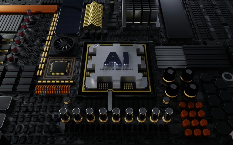
With the continuous upgrading of global electronic technology, high-speed, low-loss, high-precision multi-layer high-speed PCBs have become the core hardware carrier for artificial intelligence, cloud computing, 5G communication and industrial automation equipment.
Our integrated service portfolio covers high-speed PCB prototype, quick turn PCB production, custom high-speed PCB manufacturing, low volume PCB assembly and large-batch mass production, fully meeting demands for R&D verification, small-batch trial sales and long-term commercial supply.
With transparent capability parameters, authoritative global certifications, free professional engineering support, strict multi-level quality inspection and stable global delivery systems, we have won long-term trust from hardware engineers, procurement teams and enterprise clients worldwide.
Three Easy Ways to Start Your Project
| Option | Best For | Next Step |
|---|---|---|
| Upload Gerber Files | You have ready-made design documents | Receive detailed quotation + free DFM review within 4–8 hours |
| Contact Our Engineers | You need stackup or material selection advice | Get professional high-speed design & material optimization support |
| Request Capability Documents | You are evaluating suppliers | Obtain full factory specifications, equipment lists and certification files |
Contact our team today to discuss your high-speed PCB project. We provide free DFM inspection, customized solution evaluation and accurate quotations in the shortest time, helping your high-speed electronic products reach the market faster and more cost-effectively.