Complete Guide to High-Speed Transceiver PCBs – Material, Layout, EMI & Thermal Management
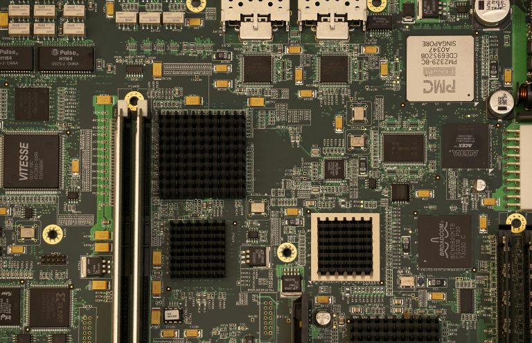
Optical modules (QSFP28, QSFP-DD, OSFP) are the backbone of modern data centers, AI clusters, and telecom networks. As speeds climb from 100G to 400G and 800G, PCB design has become the limiting factor for signal integrity, manufacturing yield, and field reliability. As detailed in the high speed PCB applications master page, optical modules represent one of the most demanding application scenarios for high-speed PCBs.
This optical module PCB guide covers everything engineers and buyers need: optical module form factors, material selection based on real data rates, 100Ω differential impedance rules, backdrilling, EMI physics, power integrity, and thermal management for high-power DSPs. The result is a complete, engineer-approved reference for optical module PCB design – suitable for hardware developers, PCB layout teams, and industrial buyers.
Why Optical Module PCB Guide Matters
Data center bandwidth doubles every 2–3 years. 400G is mainstream, 800G is ramping, and 1.6T is already in early specifications. Optical transceivers must convert electrical 100G PAM4 signals to optical and back – all inside a tiny QSFP-DD or OSFP package.
If the PCB is poorly designed, you will face:
- Eye diagram closure → high bit error rate (BER)
- PAM4 margin loss → link training failure
- EMI radiation → fails FCC/CE certification
- Overheating → DSP throttling or field failure
A correctly designed optical module PCB solves these problems through a combination of ultra-low loss materials, tightly controlled 100Ω differential pairs, backdrilling, and careful power/thermal design. This optical module PCB guide covers all these aspects in detail.
2. Optical Module Form Factors & Evolution
| Form Factor | Total Bandwidth | Electrical Lanes | Per-Lane Rate | Modulation |
|---|---|---|---|---|
| QSFP28 | 100G | 4 | 25G | NRZ |
| QSFP56 | 200G | 4 | 50G | PAM4 |
| QSFP-DD | 400G / 800G | 8 | 50G / 100G | PAM4 |
| OSFP | 400G / 800G | 8 | 50G / 100G | PAM4 |
- QSFP28 – mature, cost-effective for 100G.
- QSFP-DD – backward compatible with QSFP cages, 8 lanes.
- OSFP – slightly larger, better thermal capacity, preferred for 800G.
Modern optical module PCB design must support 56G/100G PAM4 on every lane. That forces ultra-low loss materials, 2-mil intra-pair matching, and backdrilling on every high-speed via.ckdrilling.
Core PCB Parameters for 100G / 400G / 800G
| Parameter | 100G (QSFP28) | 400G (QSFP-DD/OSFP) | 800G (QSFP-DD/OSFP) |
|---|---|---|---|
| Typical Layers | 6–8 | 8–10 | 10–12 |
| Material Grade | Low-loss | Ultra-low-loss | Ultra-low-loss |
| Differential Impedance | 100Ω ±10% | 100Ω ±10% | 100Ω ±10% |
| Intra-pair length mismatch | ≤3 mil | ≤2 mil | ≤1–2 mil |
| Max vias per lane | ≤2 | ≤2 | ≤1–2 |
| Backdrilling | Recommended | Mandatory | Mandatory |
| DSP power | 2–4W | 5–7W | 8–12W |
The trend is clear: more lanes, higher speed, tighter control, and more heat. This optical module PCB guide addresses each of these challenges.
High-Speed Material Selection & Dk/Df Grading
A key insight: a 10Gbps NRZ signal contains harmonics up to 35GHz. Df (dissipation factor) directly determines how much high-frequency energy is lost. For comprehensive Dk/Df data, refer to High-Speed PCB Material.
| Data Rate | Modulation | Material Grade | Df @10GHz Requirement |
|---|---|---|---|
| 100G (25G NRZ) | NRZ | Low-loss | <0.008 |
| 400G (50G PAM4) | PAM4 | Ultra-low-loss | <0.004 |
| 800G (100G PAM4) | PAM4 | Ultra-low-loss | <0.002 |
Rule of thumb: ≤10Gbps → mid-loss FR4; 10–28Gbps → low-loss laminate; 28–56Gbps → ultra-low-loss substrate; 56–112Gbps → ultra-low-loss + HVLP copper + strict backdrilling. For 800G modules, specify HVLP (Very Low Profile) copper foil. Standard ED copper adds significant loss at 28GHz – unacceptable for 100G PAM4. Material selection is a critical part of any optical module PCB guide.
100Ω Differential Impedance & Critical Routing Rules
All optical module high-speed lanes follow a unified 100Ω differential impedance (±10% for production, ±7% or better for 800G). This optical module PCB guide provides detailed routing rules.
5.1 100Ω Impedance Control
Impedance is determined by four physical parameters. For complete formulas, refer to Impedance Matching.
FactorEffect on Impedance Wider trace↓ lower impedance Thicker dielectric↑ higher impedance Higher Dk↓ lower impedance Larger differential gap↑ higher impedance
Always simulate with a field solver. Never rely on simple calculators for 400G/800G designs.
5.2 Length Matching & Skew
The foundational rules for Differential Pair Routing apply directly to optical module high-speed lanes.
| Speed | Intra-pair mismatch | Why |
|---|---|---|
| 25G NRZ | ≤3 mil | Moderate timing margin |
| 50G PAM4 | ≤2 mil | PAM4 eye smaller |
| 100G PAM4 | ≤1–2 mil | Extremely jitter-sensitive |
Excessive intra-pair skew directly reduces eye height and increases BER.
5.3 Serpentine & Corner Geometry
Serpentine tuning: wave height ≤ 3× trace width; spacing between segments ≥ 4× trace width. Avoid dense folding → creates crosstalk. Corners: 90° bends strictly forbidden (impedance bump + radiation); 135° chamfer acceptable for ≤10Gbps; arc/mitered bends mandatory for 25G+ and all PAM4.
5.4 AC Coupling Capacitors
Package: 100G → 0402 acceptable; 400G/800G → 0201 mandatory (reduces parasitic capacitance). Placement: near transmitter (TX) side; differential traces must remain perfectly symmetric through the capacitor. Optimization: remove copper reference plane directly under pads (anti-pad) → lowers parasitic capacitance.
5.5 Via Limits & Backdrilling
For detailed manufacturing guidelines, refer to PCB Manufacturing.
| Speed | Max vias per lane | Backdrilling |
|---|
100G≤2Recommended 400G≤2Mandatory 800G≤1–2Mandatory
Rule of thumb: Up to 10Gbps → no backdrilling; 10–20Gbps → strong recommendation; 20–40Gbps → mandatory; 40Gbps+ → backdrilling + anti-pad optimization.
5.6 Crosstalk & Tight Coupling
Keep differential gap S ≤ 2W (tight coupling) → maximizes common-mode rejection. Spacing between pairs → ≥ 4W or 20 mils. Use stripline routing (inner layers) for highest-speed lanes.
EMI Physics & Power Integrity for Optical Modules
Optical modules are extremely dense. Proper Return Path design is essential to minimize radiation. This optical module PCB guide emphasizes EMI control.
6.1 Why Small Modules Radiate
Any unbalanced differential pair produces common-mode current. Even 10-mil mismatch at 100G PAM4 creates measurable radiation. Keep intra-pair mismatch <2 mil for 400G, <1 mil for 800G. Maintain continuous ground reference – no splits under any high-speed lane.
6.2 Switching Power Supply Hot Loop
Minimize the loop area – place input capacitor very close to switching FETs. Use damping resistors on gate drives to slow down excessive ringing.
6.3 Decoupling & Plane Capacitance
Use 0201 X7R capacitors placed directly under or beside the DSP. Thin dielectric between power/ground planes creates additional plane capacitance. Several small parallel capacitors (e.g., 6× 100nF) is better than one large capacitor.
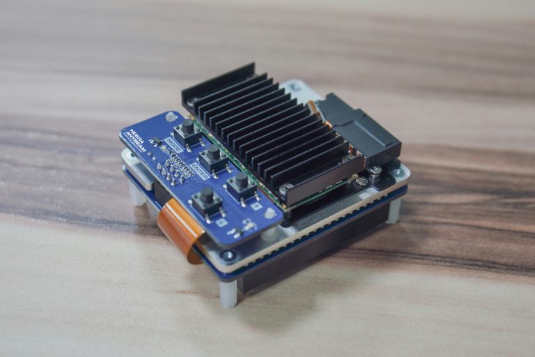
Thermal Management for High-Power DSPs
An 800G optical module DSP can dissipate 8–12W inside a package smaller than a fingernail. Proper copper thickness selection is critical for heat spreading.
| Speed | DSP Power (typical) |
|---|---|
| 100G | 2–4W |
| 400G | 5–7W |
| 800G | 8–12W |
Effective thermal design: dense thermal vias under DSP (filled or copper-plated); thick copper planes (2 oz outer, 1 oz inner); thermal pad between PCB and module cage; CFD simulation for high-power designs. Thermal management is a key focus of this optical module PCB guide.
Complete Optical Module PCB Guide Checklist
| ✅ | Item |
|---|---|
| ✅ | Material: Ultra-low-loss material for 400G/800G (Df <0.004/<0.002) |
| ✅ | Material: HVLP copper foil for all high-speed layers |
| ✅ | Impedance: 100Ω differential impedance, tolerance ≤ ±10% |
| ✅ | Routing: Intra-pair mismatch ≤3/2/1-2 mil (100G/400G/800G) |
| ✅ | Routing: Tight coupling S ≤ 2W for all differential pairs |
| ✅ | Routing: Arc corners for all 25G+ and PAM4 lanes |
| ✅ | Vias: ≤2 vias per lane (400G), ≤1–2 per lane (800G) |
| ✅ | Vias: Backdrilling applied to all 25G+ signal vias |
| ✅ | Components: AC coupling capacitors → 0201 for 400G/800G |
| ✅ | Components: Anti-pad under capacitor pads |
| ✅ | Power: Decoupling capacitors close to DSP (0201 or smaller) |
| ✅ | Power: No split ground planes under high-speed pairs |
| ✅ | Thermal: Dense thermal vias under DSP and high-power ICs |
| ✅ | Thermal: Thick copper planes (2 oz outer) |
Key Takeaways for Optical Module PCB Guide
- Optical module speed: 100G → 400G → 800G
- Material loss grade is the single most important decision: low-loss for 100G, ultra-low-loss for 400G/800G
- All high-speed lanes use 100Ω differential impedance – tolerance tightens with speed
- Backdrilling is mandatory for 400G and above
- PAM4 is extremely sensitive to mismatch, crosstalk, and discontinuities – mils matter
- EMI and power integrity are as critical as signal integrity in compact modules
- Thermal management must be designed from day one; 8–12W in a fingertip area cannot be fixed later
FAQ About Optical Module PCB Guide
Q1: What PCB material is best for 800G optical modules?
Ultra-low-loss laminates with Df <0.002 plus HVLP copper foil – a key recommendation in this optical module PCB guide.
Q2: Do I need backdrilling for 400G designs?
Yes. Backdrilling is mandatory for 25G+ lanes to eliminate via stub resonance – non-negotiable for mass production.
Q3: Can I use standard FR4 for 100G modules?
Only for extremely short traces (<2 inches). For production, low-loss material is strongly recommended.
Q4: How many vias are allowed per 100G PAM4 lane?
Maximum 2 vias; each via adds insertion loss and a small impedance bump.
Q5: How do I prevent EMI from a small QSFP-DD module?
Keep differential pairs perfectly length-matched (<2 mil); use continuous ground planes, no splits; minimize the switching power supply hot-loop area; place decoupling capacitors as close as possible to power pins.
Get Expert Support for Your Optical Module PCB Guide Project
Optical module design is no longer a simple layout task. It requires tight collaboration between signal integrity, material, thermal, and manufacturing engineering – and the right manufacturing partner.
We specialize in high-precision optical module PCBs for 100G / 400G / 800G:
- Ultra-low loss materials with precise Dk/Df control
- HVLP copper foil + tight impedance control
- Backdrilling & sequential lamination (HDI options)
- Thermal via arrays & thick copper for power delivery
- Prototype → Pilot → Mass production
📧 Send your PCB stackup, layer count and target data rate – we will provide a free technical review and a competitive custom quotation within 24 hours.
© 2026 HighSpeedPCBs