Article Abstract
High-Speed Protocol PCB Design is the foundation of reliable high-bandwidth hardware used in enterprise servers, AI accelerators, data center switches and industrial embedded devices. As signal rates climb from 8GT/s to 112Gbps with NRZ, PAM3 and PAM4 modulation, standard PCB methods no longer ensure signal integrity. This complete guide to High-Speed Protocol PCB Design delivers proven rules for PCIe 5.0 PCB design, DDR5 layout guidelines, USB4 PCB routing, 100G Ethernet PCB and SerDes PCB design to help engineers master real-world high-speed layout for mass production.
Table of Contents
- Overview of High-Speed Protocol PCB Design
- PCIe 4.0 / 5.0 / 6.0 in High-Speed Protocol PCB Design
- DDR4 & DDR5 in High-Speed Protocol PCB Design
- USB 3.2 & USB4 in High-Speed Protocol PCB Design
- 10G / 25G / 100G Ethernet in High-Speed Protocol PCB Design
- SFP+ / QSFP in High-Speed Protocol PCB Design
- SerDes & PAM4 in High-Speed Protocol PCB Design
- HDMI 2.1 in High-Speed Protocol PCB Design
- Stackup & Materials for High-Speed Protocol PCB Design
- Key Takeaways for High-Speed Protocol PCB Design
- FAQ About High-Speed Protocol PCB Design
- Design Support for High-Speed Protocol PCB Design
1. Overview of High-Speed Protocol PCB Design
High-Speed Protocol PCB Design is the core foundation of modern high-bandwidth hardware development. Unlike low-speed digital circuits, high-speed signals are extremely sensitive to trace width changes, reference plane splits, via stubs, dielectric material loss, and timing deviation. Each mainstream communication protocol is developed with unique electrical limitations, transmission distance budgets, and noise tolerance thresholds, making protocol-customized layout non-negotiable for mass production.
1.1 Why Protocol-Specific PCB Design Is Critical
Blindly applying unified high-speed routing rules across different interfaces leads to collapsed eye diagrams, severe crosstalk, signal reflection, excessive high-frequency attenuation, and frequent data transmission errors.
- Impedance standards differ: USB4 uses 90Ω differential; PCIe, Ethernet, and SerDes use 100Ω; DDR uses 40–60Ω single-ended.
- Loss budgets vary: Standard FR4 works for low-speed channels, while high-speed designs need low-loss or ultra-low-loss materials.
- Length matching is critical: Higher rates need mil-level skew control for precise timing alignment.
- Topologies are protocol-specific: DDR uses fly-by; PCIe and USB4 use point-to-point.
1.2 Protocols Covered
This guide supports all mainstream high-speed interfaces: PCIe 4.0/5.0/6.0, DDR4/DDR5, USB 3.2/USB4, 10G/25G/100G Ethernet, SFP+/QSFP, 25G/56G/112G SerDes and HDMI 2.1.
2. PCIe 4.0 / 5.0 / 6.0 in High-Speed Protocol PCB Design
PCI Express remains the dominant point-to-point high-speed interconnection for CPU, GPU, storage accelerators, and board-to-board communication. With each generation upgrade, data rates double, creating stricter requirements for impedance stability, via optimization, and high-frequency loss control.
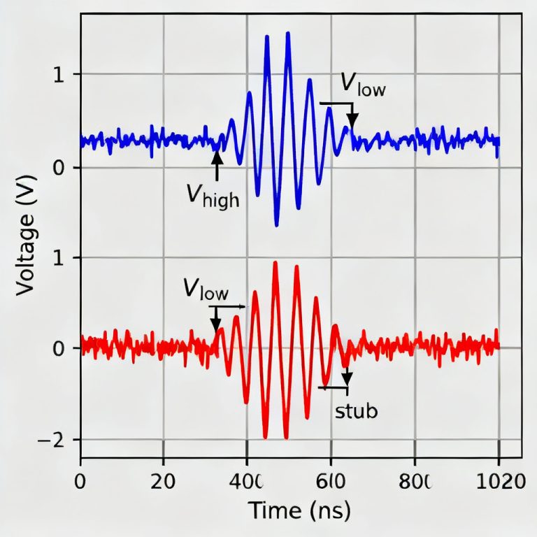
PCIe 5.0 PCB design requires strict impedance, loss control and via stub backdrill to support 32GT/s transmission.
2.1 PCIe Standard & Performance Comparison
| PCIe Generation | Data Rate | Encoding / Modulation | Material Loss Requirement |
|---|---|---|---|
| PCIe 3.0 | 8 GT/s | 128b/130b NRZ | Standard FR4 |
| PCIe 4.0 | 16 GT/s | 128b/130b NRZ | Medium-Loss FR4 |
| PCIe 5.0 | 32 GT/s | 128b/130b NRZ | Low-Loss High-Frequency Material |
| PCIe 6.0 | 64 GT/s | PAM4 | Ultra-Low-Loss Substrate |
2.2 PCIe Impedance Control
- Differential TX/RX pairs: 100Ω ±10%
- Single-end auxiliary signals: 50Ω reference impedance
2.3 PCIe Length Matching & Skew Control
| PCIe Generation | Intra-Pair Matching | Inter-Lane Matching |
|---|---|---|
| PCIe 3.0 | 5 mil | 10 mil |
| PCIe 4.0 | 5 mil | 8 mil |
| PCIe 5.0 | 2–3 mil | 5 mil |
| PCIe 6.0 | 1–2 mil | 3–5 mil |
2.4 AC Coupling Capacitor Layout
- Place coupling capacitors close to the transmitter as the preferred layout.
- Package selection: 0402 for PCIe 3.0/4.0; 0201 for PCIe 5.0/6.0 to minimize parasitic capacitance.
- Remove solid reference plane copper directly beneath capacitors to reduce resonance.
2.5 Core PCIe Layout Rules
- Crosstalk isolation: Follow the 4W–5W rule to suppress far-end crosstalk.
- Via limitation: Max 2 vias per lane.
- via stub backdrill to <10 mil for PCIe 5.0/6.0.
- Never cross ground or power plane splits for high-speed traces.
- Keep differential pairs tightly coupled with parallel routing.
2.6 PCIe Channel Insertion Loss Budget
- PCIe 4.0: <28 dB @ 8GHz
- PCIe 5.0: <36 dB @ 16GHz
- PCIe 6.0: <40 dB @ 16GHz (PAM4 with lower noise tolerance)
3. DDR4 & DDR5 in High-Speed Protocol PCB Design
DDR parallel memory interfaces involve multi-group data, address, command, and clock signals. Timing synchronization, parallel crosstalk suppression, and reasonable fly-by topology are the core challenges for reliable DDR4 and DDR5 layout.
DDR5 layout guidelines focus on timing synchronization, crosstalk isolation and fly-by topology for stable memory operation.
3.1 DDR4 vs DDR5 Core Specifications
| Memory Type | Operating Speed | VDD Voltage | Topology | Channel Feature |
|---|---|---|---|---|
| DDR4 | 1600–3200 MT/s | 1.2V | Fly-by | Single channel |
| DDR5 | 3200–6400 MT/s | 1.1V | Fly-by | Dual independent sub-channels |
3.2 DDR Impedance Requirements
- DQ / DQS data: 40–60Ω single-ended
- Differential clock CK/CK#: 100Ω
- Address & command: 40–60Ω single-ended
3.3 DDR Precise Length Matching
- DQ group intra-group: ±5 mil relative to paired DQS
- DQS differential pair intra-pair: ±2 mil
- Address / command to clock skew: ±50 mil
- DDR clock differential pair: ±2 mil
3.4 Fly-by Topology
Controller → DRAM1 → DRAM2 → DRAM3 → DRAM4 → Vtt Termination
- Clock, address and command adopt daisy-chain wiring
- DQ/DQS data use point-to-point routing
3.5 DDR Layout Best Practices
- Isolate DQ, clock and command signal groups with partitioned routing.
- Install high-density decoupling capacitors near each DRAM power pin.
- Prohibit high-frequency switching traces under DRAM chips.
- Maintain complete ground reference planes for all parallel memory signals.
4. USB 3.2 & USB4 in High-Speed Protocol PCB Design
USB is the most widely used universal high-speed interface. USB4 integrates multi-protocol SerDes transmission, bringing higher bandwidth and stricter high-speed routing limitations.
USB4 PCB routing requires tight impedance control, precise length matching and optimized connector layout for 40Gbps PAM3 transmission.
4.1 USB Generation Speed & Impedance Standard
| USB Version | Max Speed | Modulation | Differential Impedance |
|---|---|---|---|
| USB 3.2 Gen1 | 5 Gbps | 8b/10b | 90Ω |
| USB 3.2 Gen2 | 10 Gbps | 128b/132b | 90Ω |
| USB4 Gen2/Gen3 | 10–20 Gbps | 64b/66b | 90Ω |
| USB4 Gen4 | 40 Gbps | PAM3 | 90Ω |
4.2 USB Length Matching Tolerance
- USB 3.2 Gen1: 5 mil intra-pair
- USB 3.2 Gen2: 2–3 mil
- USB4 Gen3: 1–2 mil
- USB4 Gen4: 1 mil ultra-precise matching
4.3 Critical USB Layout Rules
- High-speed differential trace length controlled within 10 inches.
- Differential pair vias ≤ 2 to prevent impedance discontinuity.
- Use 45° or arc bending, avoid right angles.
- ESD devices placed close to the connector with independent ground vias.
- Strictly forbid reference plane crossing or splitting.
5. 10G / 25G / 100G Ethernet in High-Speed Protocol PCB Design
High-speed Ethernet is the backbone of data center switches, rack servers, and industrial network hardware. Backplane and midplane designs require low-loss material cooperation and multi-channel synchronous layout.
100G Ethernet PCB design demands low-loss materials, strict crosstalk control and multi-channel synchronous routing.
5.1 High-Speed Ethernet Industrial Standards
- 10GBASE-KR: 10.3125 Gbps
- 25GBASE-KR: 25.78125 Gbps
- 100GBASE-KR4: 4×25.78G NRZ channels
- 100GBASE-KP4: 4-channel PAM4 modulation
5.2 Ethernet Impedance & Skew Requirements
- High-speed SerDes differential pairs: 100Ω ±10%
- Management & control signals: 50Ω single-end impedance
- 10G: 5 mil intra-pair length matching
- 25G: 3 mil strict skew control
- 100G 4-channel: 2 mil intra-pair + inter-channel synchronization
5.3 Ethernet Layout & Topology Guidance
- Route high-speed Ethernet traces short and straight to reduce attenuation.
- Keep high-speed lanes away from crystal oscillators and switching power supplies.
- Minimize via usage; critical 100G channels recommend single-layer routing.
- Maintain fully continuous ground reference planes.
6. SFP+ / QSFP in High-Speed Protocol PCB Design
Optical module interfaces realize photoelectric conversion for data center and communication equipment. High-density connectors and high-rate SerDes signals require targeted stub reduction and impedance optimization.
SFP+ layout focuses on stub reduction, impedance continuity and crosstalk isolation.
6.1 Optical Module Specification Overview
| Module Type | Single Channel Rate | Channel Count | Total Bandwidth |
|---|---|---|---|
| SFP+ | 10 Gbps | 1 | 10 Gbps |
| QSFP+ | 10 Gbps | 4 | 40 Gbps |
| QSFP28 | 25 Gbps | 4 | 100 Gbps |
| QSFP56 | 50 Gbps (PAM4) | 4 | 200 Gbps |
| QSFP-DD | 25–100 Gbps | 8 | 400–800 Gbps |
6.2 Impedance & Length Control
- Optical high-speed differential pairs: 100Ω ±10%
- Low-speed I2C and monitoring control signals: 50Ω single-end
- 25Gbps+ interfaces: 2–3 mil intra-pair matching
- 4-channel QSFP arrays: ±5 mil inter-channel length deviation
6.3 Key Connector & Routing Rules
- Hollow reference plane copper beneath the connector to reduce stubs.
- Place AC coupling capacitors near the module side.
- Route high-speed SerDes lanes directly from controller to connector.
- Arrange ground guard vias beside signal vias.
7. SerDes & PAM4 in High-Speed Protocol PCB Design
SerDes is the physical layer foundation of all high-speed serial interfaces. The shift from NRZ to PAM4 greatly increases bandwidth but reduces noise tolerance.
SerDes PCB design requires ultra-low-loss materials, PAM4 layout rules and strict backdrilling.
7.1 SerDes Rate & Material Matching
- 25Gbps NRZ: Low-loss materials (Megtron 6, RO4350B)
- 56Gbps PAM4: Ultra-low-loss substrates (Megtron 8, RO5880)
- 112Gbps PAM4: Ceramic-filled ultra-low-loss dielectric + HVLP copper
7.2 NRZ vs PAM4 Core Differences
| Feature | NRZ Modulation | PAM4 Modulation |
|---|---|---|
| Voltage Levels | 2 | 4 |
| Eye Diagram | Single large eye | Three small eyes |
| SNR Requirement | Moderate | Very High |
| High-Loss Sensitivity | Normal | Extremely Sensitive |
7.3 SerDes Universal Layout Rules
- Fixed 100Ω differential impedance for all SerDes TX/RX lanes.
- Control typical return loss below -15dB.
- Limit via quantity and avoid multi-layer transitions for 56G/112G links.
- Isolate PAM4 channels from power and clock noise sources.
7.4 112G PAM4 Typical Channel Loss Budget
- Chip package loss: 2–3 dB
- 10-inch high-speed PCB trace loss: 10–15 dB
- Dual connector loss: 2–3 dB
- Total allowable channel loss budget: 15–25 dB
8. HDMI 2.1 in High-Speed Protocol PCB Design
HDMI 2.1 supports 8K ultra-high-definition video and high-refresh-rate display transmission, relying on high-speed TMDS differential pairs for stable video data transmission.
8.1 HDMI Version Specification
| HDMI Version | Max Rate per Channel | TMDS Channels | Differential Impedance |
|---|---|---|---|
| HDMI 1.4 | 3.4 Gbps | 3 | 100Ω |
| HDMI 2.0 | 6 Gbps | 3 | 100Ω |
| HDMI 2.1 | 12 Gbps | 4 | 100Ω |
8.2 Layout & Skew Rules
- TMDS intra-pair: 5 mil
- Inter-lane deviation: 10 mil
- Low-speed DDC and CEC signals isolated over 20 mil from high-speed lines.
9. Stackup & Materials for High-Speed Protocol PCB Design
Material and stackup choice defines the success of high-speed hardware design. All reliable systems use symmetric layer structures, controlled impedance and appropriate high-frequency materials.
9.1 High-Frequency Material Classification
| Material Grade | Application | Typical Model |
|---|---|---|
| Standard FR4 | PCIe 3.0, DDR4, 10G | IS410 |
| Medium-Loss FR4 | PCIe 4.0 | IT-170G |
| Low-Loss | PCIe 5.0, DDR5, 25G | Megtron 6, RO4350B |
| Ultra-Low-Loss | PCIe 6.0, 56G/112G PAM4 | Megtron 8, RO5880 |
9.2 Manufacturing Specification
- Symmetric stackup to prevent warpage.
- Backdrill standard: 25–40Gbps<12 mil; 40–64Gbps<10 mil; 64–112Gbps<8 mil.
- Impedance tolerance: ±10% general / ±7% for PAM4.
- 28GHz+ design requires VLP/HVLP low-roughness copper.
10. Key Takeaways for High-Speed Protocol PCB Design
- High-Speed Protocol PCB Design requires protocol-specific impedance, loss and topology rules.
- Successful implementation depends on tight length matching and symmetric routing.
- PCIe 5.0 PCB design is one of the most common demands in modern engineering.
- DDR5 layout guidelines are critical for memory stability in high-performance systems.
- USB4 PCB routing uses unique 90Ω impedance requirements.
- 100G Ethernet PCB relies on low-loss materials for long-channel reliability.
- SFP+ layout is widely used in optical communication interfaces.
- SerDes PCB design uses PAM4 layout rules as a core foundation.
- via stub backdrill is mandatory for advanced high-speed channels.
- Material selection directly determines performance and production yield.
11. FAQ About High-Speed Protocol PCB Design
Q1: What is the most important rule in High-Speed Protocol PCB Design?
A1: Impedance continuity, length matching, plane integrity and controlled loss are the four pillars of professional High-Speed Protocol PCB Design.
Q2: Why is this different from normal PCB design?
A2: It addresses signal integrity issues like reflection, crosstalk and attenuation that do not appear in low-speed designs.
Q3: Which materials are used for high-speed boards?
A3: Low-loss and ultra-low-loss materials are required for 25Gbps+ channels.
Q4: Is back-drilling required?
A4: Yes, via stub backdrill is mandatory for high-speed channels above 25Gbps.
Q5: Can standard FR4 be used for PCIe 5.0 and DDR5?
A5: No. Standard FR4 has high high-frequency loss. PCIe 5.0, DDR5 and 25G+ SerDes require low-loss or ultra-low-loss materials.
Q6: What is the standard differential impedance for high-speed interfaces?
A6: PCIe, 100G Ethernet, SerDes, SFP+ and HDMI 2.1 use 100Ω differential pairs. USB 3.2 and USB4 use 90Ω. DDR5 clock uses 100Ω differential, while data and command use 40–60Ω single-ended.
Q7: Why is precise length matching essential for high-speed signals?
A7: High-speed signals have extremely tight timing margins. Uncontrolled intra-pair skew causes signal distortion, link instability, and data errors.
Q8: What is DDR5 fly-by topology, and how is DDR5 different from DDR4?
A8: Fly-by topology is a daisy-chain routing structure for clock, address, and command signals. DDR5 introduces two independent sub-channels that must be physically isolated and not interleaved.
Q9: What makes USB4 Gen4 (PAM3) unique compared to other protocols?
A9: USB4 Gen4 uses PAM3 modulation, which has no neutral common-mode reference. It is extremely sensitive to common-mode noise, asymmetric routing, and poor component placement.
Q10: How should ESD protection grounding be designed for high-speed channels?
A10: ESD devices must use dedicated, independent ground vias. Do not share return paths with high-speed differential pairs, as this introduces noise and degrades signal quality.
12. Design Support for High-Speed Protocol PCB Design
If you need professional support for High-Speed Protocol PCB Design, our team provides end-to-end engineering services for high-speed interfaces.
We specialize in reliable, mass-production-ready layouts for industrial, server and data center hardware. Our services include free design review, stackup optimization, material selection, impedance calculation, DFM audit and customized quotation.
For professional results that ensure performance, reliability and yield, contact us today.