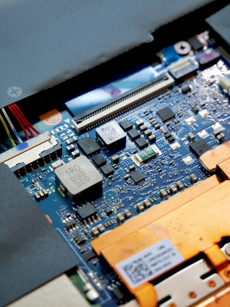
In high speed PCB design, signal integrity is paramount. One of the most debated techniques for guard traces for crosstalk reduction in high speed PCB is the use of guard traces—copper traces placed between parallel signal lines, typically connected to ground. But do guard traces really work for crosstalk reduction? This pillar page provides a definitive, evidence-based answer on guard trace effectiveness, synthesizing the most authoritative insights from leading signal integrity experts.
1. The Fundamental Physics: How Guard Traces Are Supposed to Work
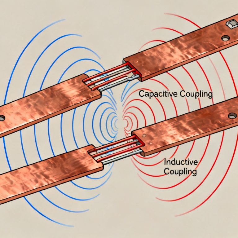
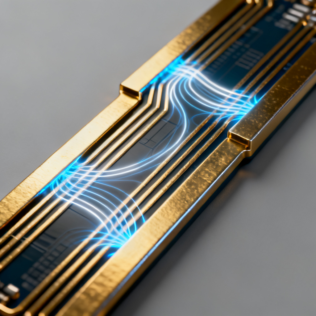
To understand if guard traces for crosstalk reduction work, we must first understand the enemy: crosstalk. Crosstalk occurs when the electromagnetic field of an “aggressor” signal line induces an unwanted voltage on a “victim” signal line. This is primarily a factor of mutual capacitance and mutual inductance between the two traces.
A guard trace, placed between the aggressor and victim, is intended to serve two functions:
- Field Containment: By placing a grounded conductor between the two lines, the guard trace provides a low-impedance return path for the electric field lines. Ideally, the guard trace “terminates” the fringe fields from the aggressor, preventing them from reaching the victim.
- Current Sinking: The guard trace intercepts the displacement current (capacitive crosstalk) and the induced current (inductive crosstalk) and shunts them directly to the ground plane, rather than allowing them to couple into the victim.
The effectiveness of this approach, however, is heavily dependent on the frequency of the signal and the distance of the guard trace to the signal lines.
2. The Critical Condition: Guard Traces Only Work When Placed Very Close
This is the single most important finding from modern signal integrity research: A guard trace is only effective if it is placed extremely close to the aggressor or victim trace.
- The Rule of Thumb: The gap between the signal trace and the guard trace (S) must be less than or equal to the height of the dielectric (H) to the reference plane. In other words,
S ≤ H. - Why? The electric field lines of a microstrip trace are concentrated within a region roughly equal to the height of the dielectric. If the guard trace is placed further away than
H, the fringe fields simply bypass the guard trace and couple directly into the victim. The guard trace becomes a decorative feature, not a functional shield. - The Practical Challenge: In a typical 4-layer PCB with a 0.2mm dielectric height, this means the guard trace must be within 0.2mm of the signal trace. This is often impossible to achieve given manufacturing tolerances and the need for other routing.
Conclusion from Top Sources: If you cannot place the guard trace within S ≤ H, do not use it for crosstalk reduction. It will provide negligible benefit while consuming valuable routing space.
3. The Stitching Via Requirement: The Most Common Mistake
Even if you place the guard trace close enough, it is completely useless if it is not properly connected to the ground plane. This is the most common and costly mistake in PCB design.
- The Problem: A floating guard trace (connected only at one end or not at all) acts as an antenna. It will actually increase crosstalk by resonating and coupling energy from the aggressor to the victim.
- The Solution: The guard trace must be stitched with vias to the ground plane at regular intervals.
- The Rule of Thumb for Via Spacing: The distance between vias along the guard trace must be less than λ/20 (where λ is the wavelength of the highest frequency component of your signal). A more practical rule is to place vias every λ/10.
- A Simpler Guideline: For digital signals, place a ground via at every point where the guard trace changes direction, and at least every 5mm to 10mm along a straight run. For RF signals, the spacing must be much tighter.
- The Consequence: Without sufficient vias, the guard trace becomes a parasitic transmission line, and its inductance dominates. It will not provide a low-impedance path to ground, and its shielding effectiveness collapses.
Conclusion from Top Sources: A guard trace without vias is worse than no guard trace at all. Always stitch it to the ground plane at intervals shorter than λ/10.

4. The Microstrip vs. Stripline Distinction
The effectiveness of guard traces varies dramatically depending on the routing layer.
- Microstrip (Outer Layers): This is where guard traces have the most potential to help. Because the fields are exposed to air on one side, the fringing fields are more extensive. A well-placed and well-stitched guard trace can significantly reduce capacitive crosstalk. However, inductive crosstalk reduction is minimal.
- Stripline (Inner Layers): This is where guard traces are almost never effective. Because the signal is already sandwiched between two solid ground planes, the fields are tightly confined. The primary crosstalk in stripline is inductive, and a guard trace does little to reduce mutual inductance. In fact, the guard trace can actually increase mutual inductance by creating a “slot” in the return current path.
Conclusion from Top Sources: Guard traces are a viable (but difficult) option for microstrip. For stripline, they are generally a waste of time. Focus on other techniques like increasing trace spacing or using differential signaling.
5. The Real-World Performance: What the Data Shows
Signal integrity engineers have run countless simulations and measurements. Here is the consensus on actual performance:
- Capacitive Crosstalk (Near-End): A properly designed guard trace (close, stitched) can reduce near-end crosstalk by 30% to 50% in microstrip. This is a meaningful improvement.
- Inductive Crosstalk (Far-End): Guard traces provide very little to no reduction of far-end crosstalk. This is because inductive coupling is a magnetic field phenomenon, and a grounded copper trace does not effectively block magnetic fields.
- The “Stitching” Effect: The biggest benefit of a guard trace often comes not from the trace itself, but from the vias. The row of ground vias acts as a “wall” that breaks up the fringe fields. If you can place a row of ground vias between the aggressor and victim without a connecting trace, you will get better performance than with a guard trace alone.
Conclusion from Top Sources: The vias are more important than the trace. A row of ground vias without a guard trace can be more effective than a guard trace with insufficient vias.
6. The Alternatives: What Works Better Than Guard Traces
Given the difficulty of implementing guard traces correctly, what are the proven alternatives?
- 1. Increase Trace Spacing (The Most Reliable Method): This is the single most effective and easiest way to reduce crosstalk. Doubling the distance between traces reduces crosstalk by approximately 50% (6dB). The industry standard “3W rule” (spacing = 3x trace width) is a good starting point, but for high-speed signals, 5W or more may be required.
- 2. Reduce the Dielectric Height (H): Bringing the signal layer closer to the ground plane tightly confines the fields, reducing both capacitive and inductive coupling. This is a fundamental stack-up design choice.
- 3. Use Differential Signaling: Differential pairs are inherently immune to common-mode crosstalk. The tight coupling between the + and – signals means that external noise couples equally to both, and the receiver rejects it.
- 4. Route on Different Layers: If you have the layer count, simply route critical high-speed signals on different layers, separated by a ground plane. This provides perfect isolation.
- 5. Use a Ground “Fence” (Via Wall): Instead of a guard trace, place a row of ground vias between the aggressor and victim. This creates a virtual Faraday cage and is often more effective than a guard trace, especially at higher frequencies.
7. When Should You Actually Use Guard Traces?
Given all the caveats, are there any scenarios where guard traces are the right choice?
- Scenario A: You have a very tight constraint. You cannot increase trace spacing due to board size limitations, and you are routing microstrip. You are willing to sacrifice routing channel density.
- Scenario B: You are an expert designer. You understand the physics, you can calculate the required via spacing (λ/20), and your PCB manufacturer can achieve the tight trace-to-guard spacing (S ≤ H).
- Scenario C: You are mixing analog and digital. In mixed-signal designs (e.g., a sensitive ADC next to a high-speed digital bus), a guard trace between the two sections, stitched to a solid ground plane, can help prevent digital noise from coupling into the analog domain. This is a common and effective use case.
8. Final Verdict: Do Guard Traces Really Work?
The answer is: Yes, but only under very specific and difficult-to-achieve conditions.
- They work for reducing capacitive crosstalk in microstrip when placed within S ≤ H and stitched with vias at λ/10 intervals or less.
- They do not work for reducing inductive crosstalk.
- They do not work in stripline.
- They are counterproductive if left unstitched (increasing crosstalk).
The Practical Advice for 99% of Designs: Do not use guard traces. Instead, increase trace spacing and optimize your stack-up. These methods are simpler, more reliable, and more effective. If you must use guard traces, treat them as a last resort and simulate your design thoroughly.
Frequently Asked Questions About Guard Traces for Crosstalk Reduction
What is a guard trace in high speed PCB design?
A guard trace is a grounded copper trace placed between signal lines to reduce crosstalk in high speed PCB layouts. It works by providing a low-impedance path for interfering fields.
Do guard traces reduce crosstalk effectively?
Guard traces for crosstalk reduction are effective only when placed very close to the signal lines (S ≤ H) and stitched with vias at proper intervals. Without these conditions, they offer little benefit.
What is the difference between microstrip and stripline guard traces?
In microstrip (outer layers), guard traces can reduce capacitive crosstalk if properly designed. In stripline (inner layers), they are generally ineffective due to the confined fields and dominant inductive coupling.
What are the best alternatives to guard traces?
The most reliable alternatives include increasing trace spacing, reducing dielectric height, using differential signaling, routing on separate layers, and employing ground via fences.
Guard Traces vs. Alternatives: Performance Comparison
| Technique | Crosstalk Reduction (Capacitive) | Crosstalk Reduction (Inductive) | Implementation Difficulty | Recommended Use Case |
|---|---|---|---|---|
| Guard Trace (Microstrip, S ≤ H, stitched) | 30-50% | Minimal | High | Last resort, tight spacing |
| Guard Trace (Stripline) | Negligible | Negligible | High | Avoid |
| Increase Trace Spacing (3W rule) | ~50% per doubling | ~50% per doubling | Low | Primary method |
| Reduce Dielectric Height (H) | Significant | Significant | Medium | Stack-up optimization |
| Differential Signaling | High (common-mode rejection) | High | Medium | High-speed data lines |
| Ground Via Fence | High | Moderate | Medium | Isolation between sections |
Key Terminology for High Speed PCB Design
- Crosstalk: Unwanted electromagnetic coupling between adjacent signal traces, a primary concern in high speed PCB design.
- Guard Trace: A grounded conductor placed between signal lines to reduce crosstalk, often used in high speed PCB layouts.
- Microstrip: A transmission line on the outer layer of a PCB, with one side exposed to air.
- Stripline: A transmission line embedded between two ground planes, common in multilayer PCBs.
- Stitching Via: A via connecting the guard trace to the ground plane, essential for effective crosstalk reduction.
- Dielectric Height (H): The thickness of the insulating layer between the signal trace and the reference plane, affecting field confinement.
Need Expert Help with Your High-Speed PCB? At [Your Company Name], we specialize in the design and fabrication of high-speed PCBs where signal integrity is non-negotiable. Our engineering team can review your stack-up, routing strategy, and crosstalk mitigation plan to ensure first-pass success. Contact us today for a free design review or to request a quote for your next high-speed PCB project.