Plane pair resonance in a power integrity PCB is a critical electromagnetic phenomenon that corrupts the power distribution network (PDN) at high frequencies. This guide explains its causes, effects, and proven mitigation techniques for high-speed PCB design.
What Is Plane Pair Resonance in Power Integrity PCB?
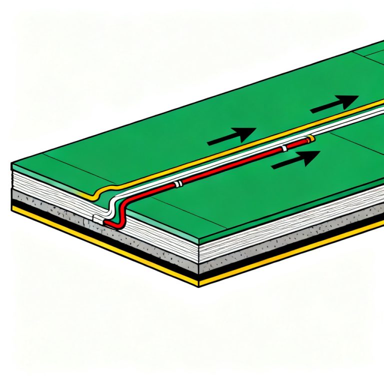
The Parallel-Plate Waveguide Model
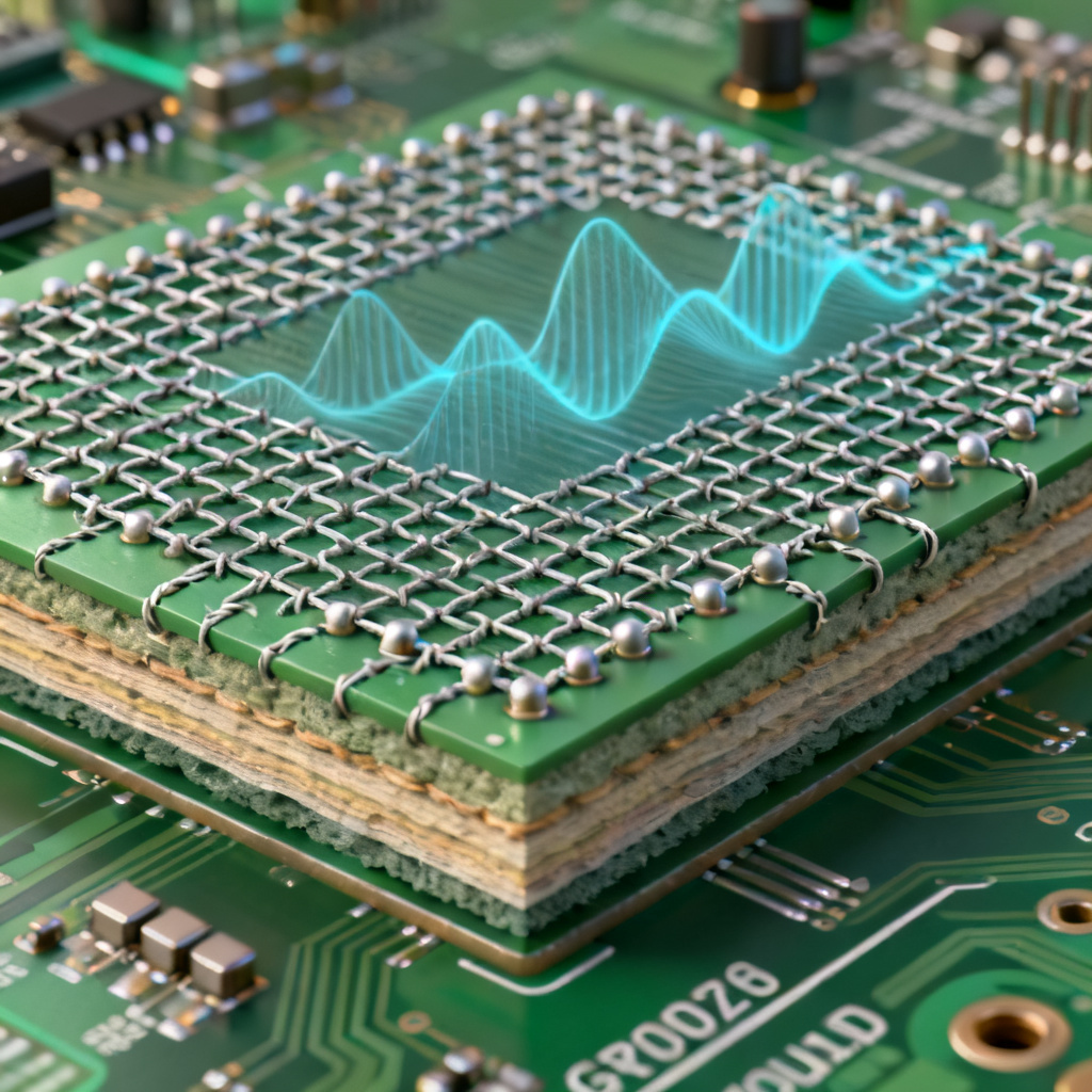
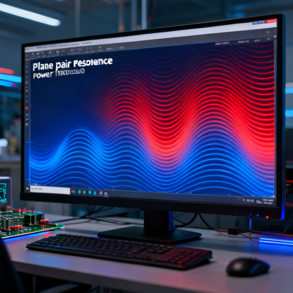
Plane pair resonance is a major concern for Power Integrity PCB. It occurs when the power and ground planes (VCC and GND) form a parallel-plate waveguide. This waveguide supports TEM and TM wave propagation. At low frequencies, the plane pair behaves as a large capacitor, providing low impedance. At high frequencies, the inductive loop dominates, and the planes become resonant cavities. When the electrical length equals a multiple of half-wavelength (λ/2) or quarter-wavelength (λ/4), a standing wave pattern forms. This is plane pair resonance, which further deteriorates the power integrity performance of PCBs.
Cavity Resonance Modes
Resonance modes are defined by plane dimensions (length a, width b) and dielectric constant (εr). The resonant frequency for a rectangular cavity is: f_mn = (c / (2π√εr)) * √((mπ/a)² + (nπ/b)²). Common modes include TM01 (voltage maximum at one axis center), TM10 (maximum at the other axis center), and higher-order modes (TM11, TM21, etc.) with multiple voltage maxima and minima. Plane pair resonance frequency is inversely proportional to plane dimensions.
Role of Dielectric Thickness
The separation distance (h) between planes is critical. A thicker dielectric increases loop inductance, lowering the self-resonant frequency. For high-speed PDN design, thin dielectrics (e.g., 2-4 mils) are preferred to increase plane capacitance and push plane pair resonance to higher, less problematic frequencies. However, thin dielectrics also reduce damping, increasing risk.
Effects of Plane Pair Resonance on Power Integrity PCB
Impedance Spikes at Resonant Frequencies
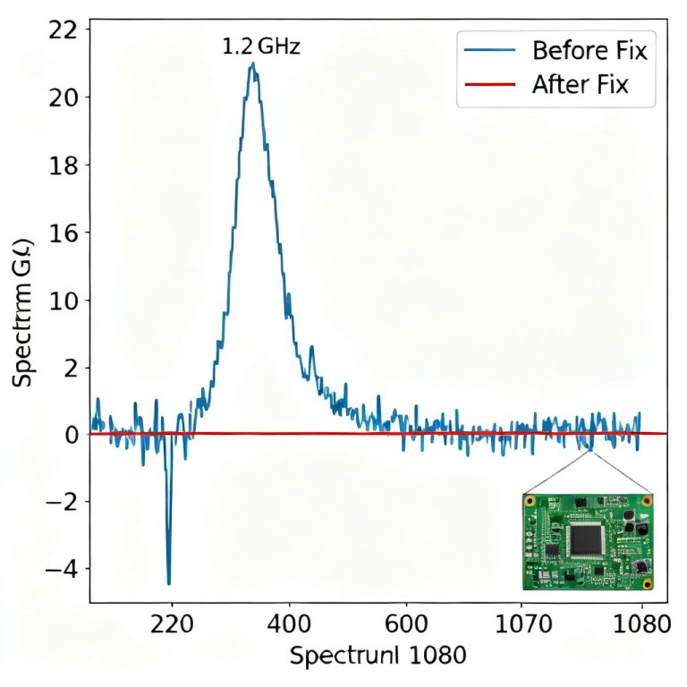
The most direct effect of plane pair resonance is a dramatic impedance increase at resonant frequencies. An ideal PDN should maintain target impedance (e.g., < 1 mΩ) across all frequencies. At resonance, impedance can spike to tens or hundreds of ohms. When an IC draws transient current, the voltage drop V_drop = I_transient * Z_PDN causes significant voltage ripple, violating IC voltage tolerance and causing logic errors.
Increased Simultaneous Switching Noise (SSN)
Plane pair resonance amplifies ground bounce and power supply noise when multiple output drivers switch simultaneously. This is severe in high-speed parallel buses (e.g., DDR memory interfaces). The resonant cavity couples noise from a switching driver to a quiet receiver, causing false triggering.
Electromagnetic Interference (EMI) Radiation
A resonant plane pair acts as an efficient antenna. Standing waves create high-frequency currents that flow to board edges. At resonance, voltage maximum occurs at the edges, creating a strong electric field that couples to cables or enclosures, causing radiated emissions that fail FCC or CE compliance.
Degraded Signal Integrity via Return Path Discontinuity
Plane pair resonance disrupts return current paths for high-speed signals. A signal trace over a resonant plane pair sees varying impedance. The return current, which should flow directly under the trace, is forced through the resonant cavity, increasing loop area, creating common-mode noise, and increasing crosstalk. For differential pairs, plane pair resonance causes mode conversion.
Mitigation Strategies for Plane Pair Resonance in Power Integrity PCB
Strategic Decoupling Capacitor Placement
Decoupling capacitors (decaps) provide a low-impedance path at their self-resonant frequency. To combat plane pair resonance, decaps must be placed at anti-nodes (points of maximum voltage fluctuation). Simulation using 2D/3D EM solvers (e.g., Ansys SIwave, Cadence Sigrity) is essential to identify voltage hot spots. Place decaps near IC power pins and distribute them across the board, especially near corners and edges. Use a mix of values (1 nF, 10 nF, 100 nF, 1 µF) to cover a broad frequency range.
Via Stitching and Via Fences
Vias between power and ground planes act as short-circuit posts, altering resonant frequencies and damping modes. Via stitching adds a grid of vias connecting the planes, with spacing less than λ/20 at the highest frequency of concern. For a 5 GHz resonance (λ ≈ 60 mm in FR4), via spacing should be < 3 mm. Via fences surround sensitive areas (e.g., a high-speed IC) to create a local cavity. Vias increase effective capacitance and reduce loop inductance, raising the resonant frequency and damping impedance peaks.
Plane Cutouts and Slots (Use with Caution)
Cutting slots or removing copper can disrupt the resonant cavity. Use slots to isolate noisy digital regions from sensitive analog/RF areas. However, slots create return path discontinuities, worsening SI and EMI, and can create new lower-frequency resonances. Only use cutouts as a last resort, verified by simulation.
Optimizing Layer Stackup and Dielectric Thickness
Use the thinnest possible dielectric between power and ground planes (e.g., 2-4 mils). This increases plane capacitance and raises resonant frequencies, often pushing them above the operating frequency. Use multiple VCC-GND plane pairs to create parallel capacitance, lowering overall PDN impedance. For high-frequency applications, use low-loss dielectrics (e.g., Rogers, Megtron) instead of FR4, which becomes unreliable above 1 GHz.
Lossy Materials (Absorbers)
For extreme cases, thin magnetic or dielectric absorber sheets can be placed between the plane pair or on the board surface. Absorbers convert EM energy into heat, damping plane pair resonance. Drawbacks include added cost, thickness, and thermal management issues. Typically used in military, aerospace, or high-end telecom designs.
Embedding Capacitance (Buried Capacitance)
Use a thin layer of high-dielectric-constant material between power and ground planes. This creates distributed, low-inductance capacitance that suppresses plane pair resonance across a wide frequency range. Advantages include extremely low inductance (no via inductance), wideband suppression, and reduced component count. Disadvantages include higher board cost and limited availability.
Simulation and Measurement for Plane Pair Resonance Verification
Simulation Tools
Use full-wave EM simulation to identify resonant frequencies, mode shapes, and voltage hot spots. Optimize decap placement and via stitching patterns. Evaluate the impact of cutouts or stackup changes. Tools include Ansys SIwave, Cadence Sigrity, and Keysight ADS.
Measurement Techniques
Use a VNA to measure S-parameters (S21) across the plane pair; a dip in S21 indicates a resonant mode. TDR/TDT reveals impedance discontinuities caused by plane pair resonance. Near-field scanning with a magnetic field probe maps the standing wave pattern on the board surface.
Design Guidelines for B2B High-Speed PCB Manufacturing
As a manufacturer, guide clients to avoid plane pair resonance pitfalls. Provide these recommendations in technical documentation:
- Request a PDN impedance simulation before fabrication.
- Specify a thin core (e.g., 2116 or 1080 prepreg) for the VCC-GND plane pair.
- Require via stitching on all large plane areas, with spacing < 3 mm for designs above 5 GHz.
- Advise against unnecessary plane cutouts unless verified by simulation.
- Use a mix of decoupling capacitor values (0402 or 0201 packages for low inductance) placed at simulated anti-nodes.
- Consider embedded capacitance for ultra-high-speed designs (e.g., 25 Gbps+).
Frequently Asked Questions About Plane Pair Resonance in Power Integrity PCB
What is plane pair resonance in a power integrity PCB?
How does plane pair resonance affect power integrity?
What are the best mitigation techniques for plane pair resonance?
Comparison: Plane Pair Resonance Mitigation Techniques for Power Integrity PCB
| Mitigation Technique | Effectiveness Against Plane Pair Resonance | Cost Impact | Design Complexity |
|---|---|---|---|
| Decoupling Capacitor Placement | High (when placed at anti-nodes) | Low | Medium |
| Via Stitching | High (damps modes) | Low | Low |
| Thin Dielectric Stackup | High (raises resonant frequency) | Low | Low |
| Embedded Capacitance | Very High (wideband suppression) | High | Medium |
| Lossy Absorbers | High (damps resonance) | High | Low |
Key Terms in Plane Pair Resonance for Power Integrity PCB
- Plane pair resonance: The formation of standing waves between power and ground planes at specific frequencies.
- Power distribution network (PDN): The system delivering stable voltage to ICs, including planes, decaps, and vias.
- Anti-node: A point of maximum voltage fluctuation in a standing wave pattern, where decaps are most effective.
- Via stitching: Adding vias connecting power and ground planes to dampen resonance.
- Embedded capacitance: A thin high-Dk layer between planes for wideband noise suppression.