In high-speed PCB design, the Return Path for Microstrip vs Stripline follows fundamentally different rules. For every signal current flowing from driver to receiver, an equal and opposite current must return. If this path is disrupted, the trace becomes an unintentional antenna, radiating EMI and degrading signal integrity.
The Physics of the Return Path: Why It Differs for Microstrip vs Stripline
Understanding the Return Path for Microstrip vs Stripline begins with high-frequency physics. At DC, current spreads across the entire ground plane. At high frequencies, the return current concentrates directly under (or above) the signal trace, following the path of minimal loop area due to mutual inductance. This principle governs every design rule for Return Path PCB Design for Microstrip vs Stripline.
Why Impedance Dictates Return Path Behavior
The Return Path for Microstrip vs Stripline differs because of impedance. For microstrip, the return current flows on a single reference plane below, with fields partially in air and substrate. For stripline, the return current splits equally between two planes, creating a balanced field. This impacts EMI, crosstalk, and propagation delay.
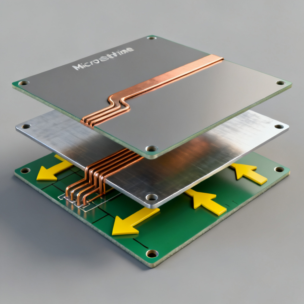
Microstrip Return Path Rules: Single Plane Discipline
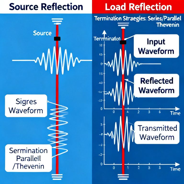
A microstrip trace sits on an outer layer with one reference plane below. The Return Path for Microstrip vs Stripline here requires never breaking that plane. A slot or gap forces the return current into a long detour, creating a radiating loop. Use stitching capacitors near transitions between GND and VCC planes to maintain a low-impedance path.
Ground Flooding and Stitching Vias
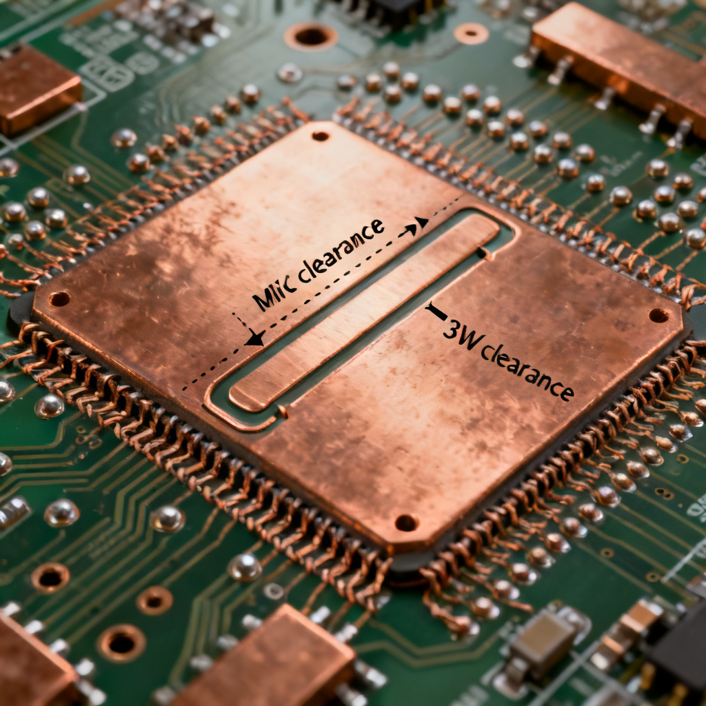
For microstrip, surround the trace with ground copper on the same layer, connected to the plane with dense stitching vias. This creates a coaxial-like environment. Maintain 3W to 5W clearance from trace to flood to preserve controlled impedance. Place vias no more than 1/10th wavelength apart for effective Return Path continuity.
Avoiding Surface-Level Discontinuities
Microstrip fields fringe into air, making them sensitive to board edges and copper pours. Keep high-speed traces away from board perimeters. Use 45-degree chamfers instead of 90-degree corners to prevent field concentration and impedance variation.
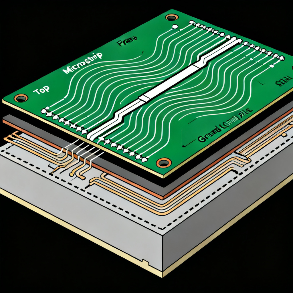
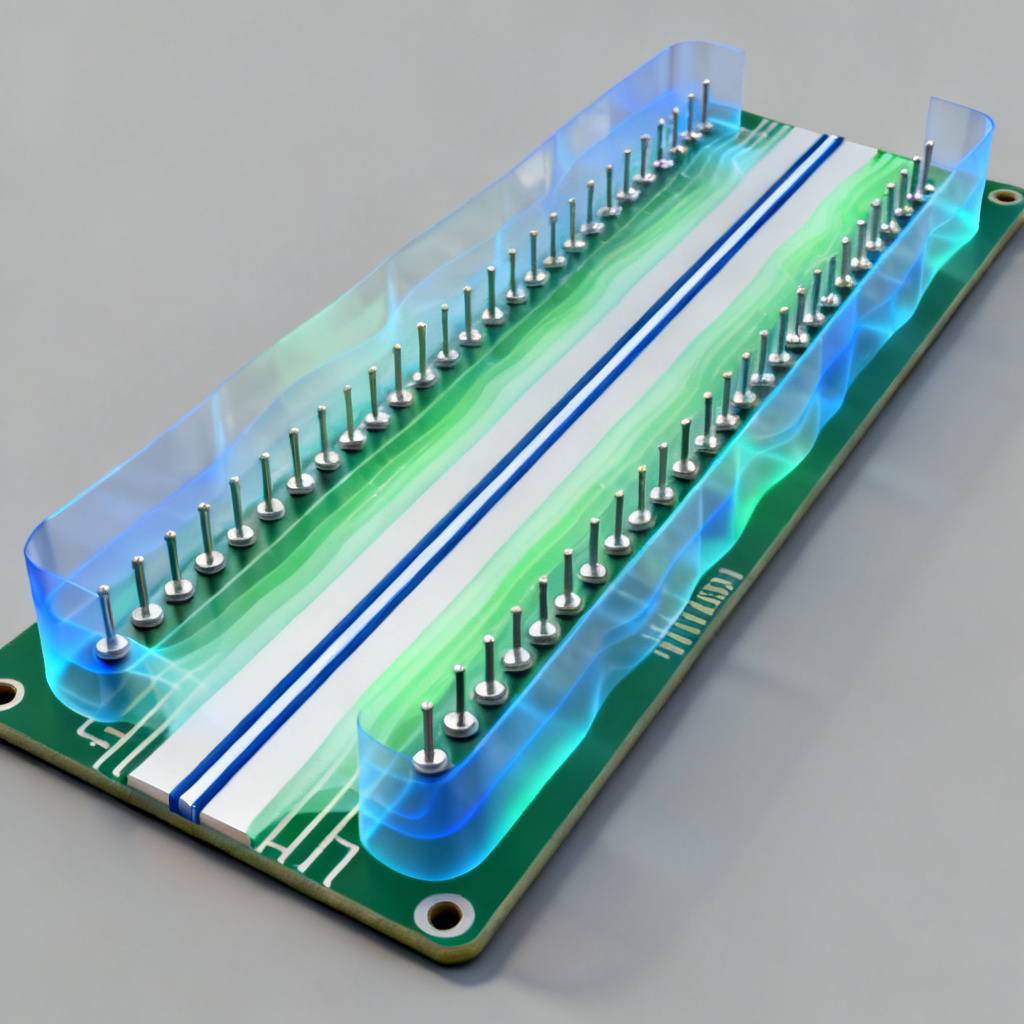
Stripline Return Path Rules: Dual Plane Balance
A stripline trace sits between two solid reference planes. The Return Path for Microstrip vs Stripline here splits 50% above and 50% below. This requires AC-connecting both planes with stitching vias around the stripline region. Without these vias, the structure becomes asymmetrical, losing its EMI shielding advantage.
Via Fencing for Ultra-High-Speed Signals
For 10 Gbps+ designs, use a via fence—a row of closely spaced ground vias along the trace length. This creates a quasi-coaxial structure, fully containing the electromagnetic field and isolating sensitive signals from crosstalk.
Avoiding Plane Splits in the Cavity
If the two reference planes are different voltage domains (e.g., 1.8V and 3.3V), ensure capacitive coupling with decoupling capacitors. The safest practice is to always use solid GND planes as primary references for stripline layers, even if power planes exist on adjacent layers.
Comparative Table: Return Path for Microstrip vs Stripline
| Parameter | Microstrip Return Path | Stripline Return Path |
|---|---|---|
| Reference Planes | Single plane below | Two planes above and below |
| EMI Susceptibility | High (exposed to noise) | Low (shielded by planes) |
| Propagation Delay | Faster (~140-150 ps/inch) | Slower (~170-180 ps/inch) |
| Crosstalk Level | Higher (fields fringe into air) | Lower (fields confined) |
| Key Design Rule | Never cut ground plane below | Stitch top and bottom planes |
| Best Use Case | Low-cost, short traces, RF | Critical clocks, data buses, analog |
Common Violations and Fixes for Return Path
Violation 1: A void in the ground plane under a microstrip trace (e.g., via anti-pad). Fix: Minimize anti-pad size; never route over it. Violation 2: A microstrip trace crossing from GND to VCC plane. Fix: Place a stitching capacitor within 100 mils of the crossing. Violation 3: Unstitched stripline planes. Fix: Add via fence every 1/10th wavelength.
Expert Tips for Optimal Return Path Design
For microstrip, always maintain continuous ground flooding and dense stitching vias. For stripline, ensure both planes are AC-connected. In mixed designs, use microstrip for short, low-speed traces and stripline for all critical high-speed signals (DDR, PCIe, SerDes). This hybrid approach optimizes both cost and signal integrity.
FAQ: Return Path PCB Design for Microstrip vs Stripline
What is the main difference in return path between microstrip and stripline?
The Return Path for Microstrip vs Stripline differs in reference planes. Microstrip uses a single plane below, while stripline uses two planes above and below, with current splitting 50/50. This affects EMI, crosstalk, and design rules.
How do I fix a broken return path in microstrip?
Place stitching capacitors near transitions between GND and VCC planes. Ensure continuous ground flooding and use stitching vias no more than 1/10th wavelength apart to maintain a low-impedance Return Path.
Why is stripline better for high-speed signals?
Stripline provides a shielded Return Path with two reference planes, reducing EMI and crosstalk. It is ideal for critical high-speed interfaces like PCIe, DDR, and SerDes.
What is via fencing and when should I use it?
Via fencing is a row of closely spaced ground vias along a stripline trace. Use it for 10 Gbps+ signals to create a quasi-coaxial structure that fully contains the electromagnetic field and isolates crosstalk.
Can I mix microstrip and stripline in the same design?
Yes. Use microstrip for short, low-cost traces and stripline for critical high-speed signals. Ensure proper transition vias and stitching capacitors to maintain Return Path continuity between layers.