To simulate reflection in transmission line using Ansys HFSS is essential for signal integrity in high-speed PCB design. This guide provides a complete workflow for accurate electromagnetic simulation.
Introduction to Reflection in Transmission Line Simulation
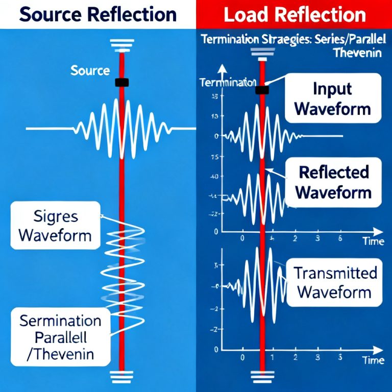
Reflection in transmission line occurs when an electromagnetic wave encounters an impedance discontinuity, such as at connectors, vias, or bends. In high-speed digital circuits, even small reflections cause signal distortion. Using Ansys HFSS to simulate reflection in transmission line allows you to predict S11 parameters, visualize field patterns, and optimize impedance matching before fabrication.
Prerequisites for Simulating Reflection in Transmission Line
Before simulating reflection in transmission line using Ansys HFSS, ensure you have Ansys HFSS installed (version 2021 R1 or later), basic knowledge of transmission line theory, a PCB stackup with defined materials, and simulation goals like target frequency or bandwidth.
Step-by-Step Guide to Simulate Reflection in Transmission Line Using Ansys HFSS
Step 1: Define the Transmission Line Geometry
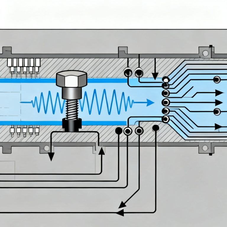
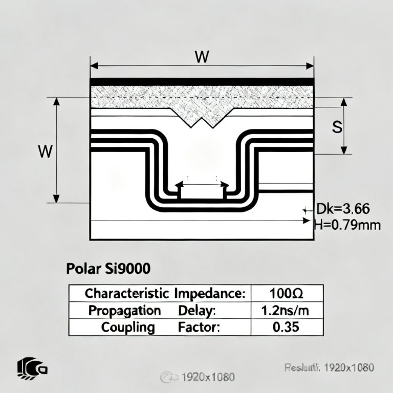
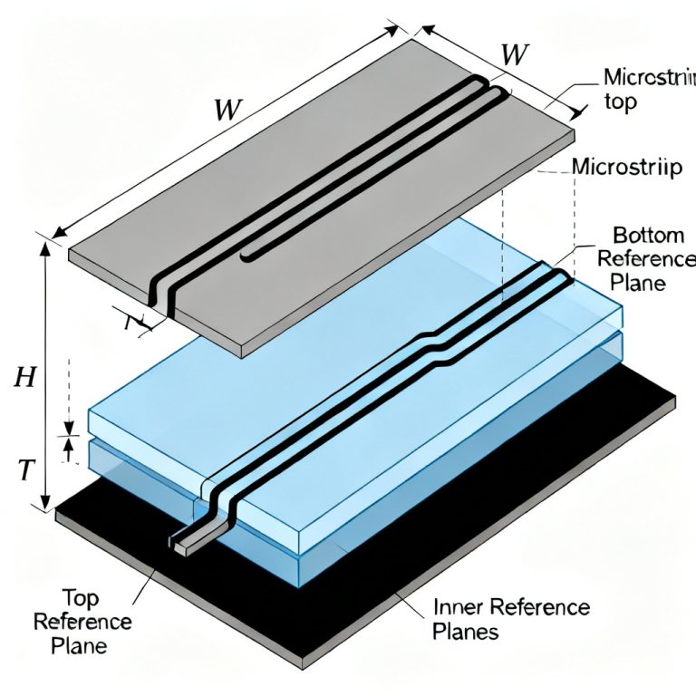
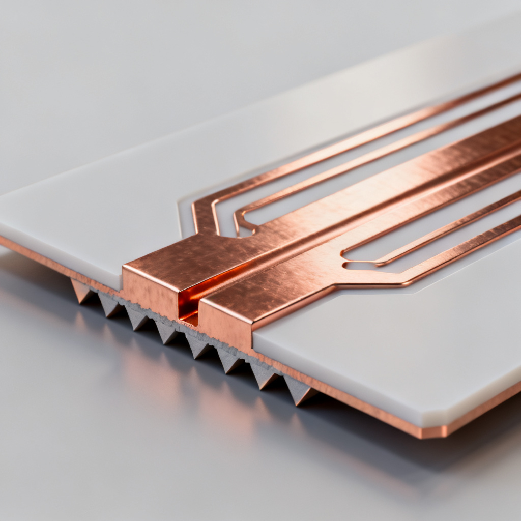
Open HFSS and create a new project. Use the 3D Modeler to draw a transmission line trace, such as a microstrip on a substrate. Define the substrate as a box with FR4 material (εr=4.4, loss tangent=0.02). Draw the copper trace as a rectangular sheet (thickness 0.035 mm, conductivity 5.8e7 S/m). Add a ground plane below the substrate. Assign materials from the HFSS library, set “Perfect E” boundary for the ground plane, and “Finite Conductivity” for the trace.
Step 2: Configure Ports and Excitations for Reflection Analysis
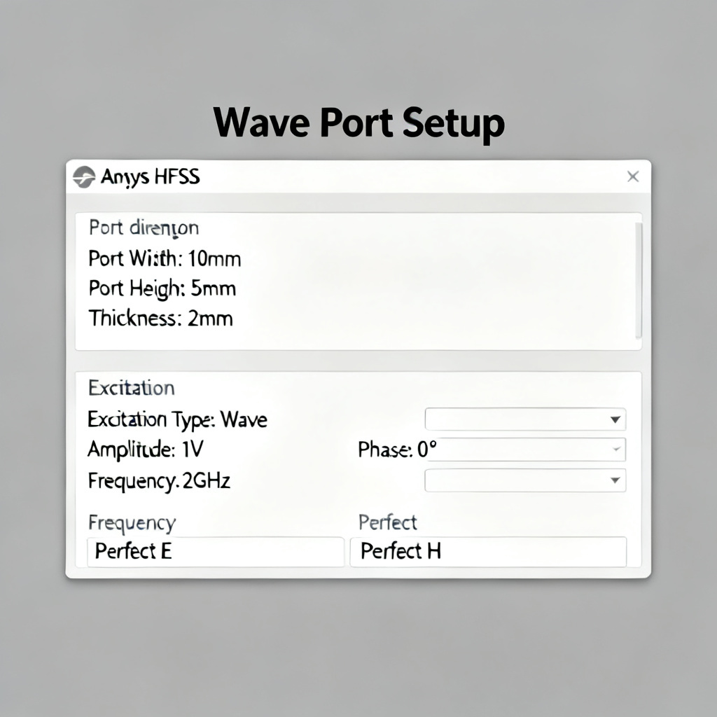
Create wave ports at the input and output ends of the transmission line. Ensure port size is 5 times the trace width on each side and 3-5 times the substrate height above. Assign “Wave Port” excitation to each port. For reflection analysis, focus on Port 1 as source and Port 2 as load. Set reference impedance to 50 ohms in port properties.
Step 3: Set Up the Simulation for Transmission Line Reflection
In the Analysis tab, add a solution setup with “Solution Frequency” at your target (e.g., 10 GHz) or a range (1-20 GHz). Set adaptive mesh with “Maximum Number of Passes” to 10-15 and “Delta S” criterion of 0.01. Add an “Interpolating Sweep” with step size 0.1 GHz for broadband results.
Step 4: Run the Simulation
Validate the model using “Modeler > Validate” to check for geometric errors. Click “Analyze” to start the solver. Monitor convergence in the Message Manager. Typical simulation time is 5-30 minutes depending on complexity.
Step 5: Analyze Reflection Results
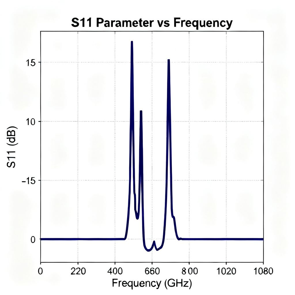
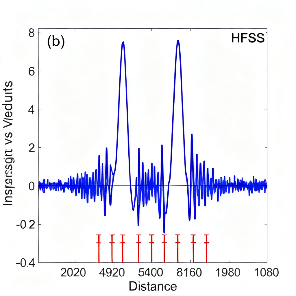
After simulation, go to “Results > Create Modal Solution Data Report > Rectangular Plot”. Select S-Parameter and plot S11 (reflection coefficient) and S21 (transmission coefficient) in dB. For reflection, S11 below -10 dB indicates good impedance matching. Use “Field Overlays” to plot E-field and identify standing wave patterns. Convert S-parameters to TDR for impedance vs. distance analysis.
Step 6: Optimize Design to Reduce Reflection
From TDR plots, locate impedance mismatches at bends, vias, or connector pads. Adjust trace width to achieve target impedance (e.g., 50 ohms for microstrip). Add chamfered corners and via stitching. Re-simulate to verify improvement, aiming for S11 below -20 dB.
Advanced Techniques for Accurate Reflection Simulation
Using De-Embedding for Accurate Port Results
Use “De-Embedding” in HFSS to remove parasitic effects from ports. Set “De-Embed Distance” to the feed line length in port properties. This improves accuracy for short transmission lines.
Modeling Lossy Materials
For FR4, include dielectric loss (tanδ) and conductor roughness using the “Groisse” model. This enhances accuracy for high-frequency reflection above 5 GHz.
Simulating Differential Pairs
For differential signals like USB or HDMI, create two traces with a defined gap. Use “Differential Ports” to analyze common-mode and differential-mode reflections (Sdd11, Scc11).
Parametric Sweeps for Optimization
Use “Optimetrics” to sweep parameters like trace width, substrate height, or dielectric constant. This identifies optimal geometry for minimal reflection.
Common Pitfalls and Troubleshooting
Port size too small: Leads to inaccurate S-parameters. Ensure ports extend 3-5 times substrate height beyond trace edges. Mesh convergence failure: Increase “Maximum Number of Passes” or refine mesh manually near high-field gradients. Unrealistic material models: Use measured data for FR4 at high frequencies. Ignoring radiation losses: Enable “Radiation Boundary” on top and sides of the air box for microstrip structures.
Case Study: Simulating Reflection in a High-Speed Microstrip Line
Design: 50-ohm microstrip on FR4 (εr=4.4, height 0.2 mm, trace width 0.38 mm, length 100 mm). Simulation in HFSS with frequency sweep 1-10 GHz. Results: S11 at 5 GHz was -12 dB. TDR showed impedance drop at 45 mm due to a via pad. Optimization: Increased trace width to 0.42 mm near the via. Re-simulation gave S11 of -25 dB. This demonstrates how to simulate reflection in transmission line using Ansys HFSS effectively.
Frequently Asked Questions
What is the best way to simulate reflection in transmission line using Ansys HFSS?
Follow the step-by-step process above: define geometry, configure wave ports, set up adaptive mesh, run simulation, and analyze S11 parameters.
How accurate is HFSS for transmission line reflection simulation?
HFSS provides high accuracy when port sizes, material models, and mesh settings are properly configured. Use de-embedding and lossy material models for best results.
Can I simulate differential pair reflection in HFSS?
Yes, use “Differential Ports” to analyze Sdd11 and Scc11 parameters for differential transmission lines.
Conclusion
Simulating reflection in transmission line using Ansys HFSS is critical for high-speed PCB design. By following this guide, you can model, analyze, and optimize designs to achieve low reflection (S11 below -20 dB), ensuring signal integrity in applications like 5G, data centers, and automotive electronics. Practice with simple geometries first, then apply to complex multilayer boards.
Transmission Line Reflection Simulation Parameters Table
| Parameter | Value | Impact on Reflection |
|---|---|---|
| Target Impedance | 50 ohms | Matching reduces reflection |
| Trace Width | 0.38 mm | Wider trace lowers impedance |
| Substrate Height | 0.2 mm | Thinner substrate increases impedance |
| Dielectric Constant | 4.4 | Higher Dk reduces impedance |
Glossary of Key Terms
Reflection coefficient (S11): Ratio of reflected to incident voltage, expressed in dB. Impedance discontinuity: Any change in characteristic impedance along a transmission line. TDR: Time Domain Reflectometry, used to measure impedance vs. distance.