Article Abstract
This ultimate serdes pcb design guide delivers industry-standard routing rules, channel loss budget allocation, PCB material grading, impedance control, via optimization, backdrilling requirements, and PAM4-specific layout considerations for 25G NRZ, 28G NRZ, 56G PAM4, and 112G PAM4 applications. Compiled from top EDA vendors, electronic engineering media, and global high-speed design service benchmarks, this serdes pcb design guide balances professional technical depth for hardware and layout engineers while remaining easy to follow for procurement and project managers. It covers complete design workflows, comparison tables, layout checklists, common pitfalls, and actionable best practices for data center switches, servers, AI accelerators, and backplane systems.
Overview of SerDes PCB Design Guide
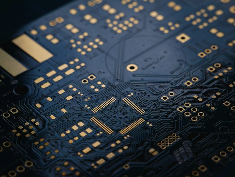
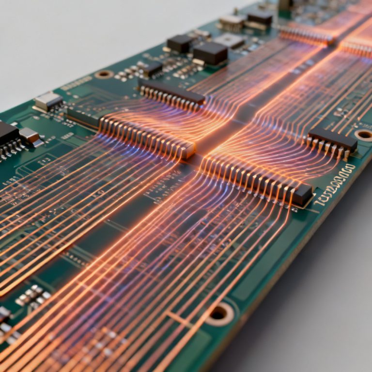
Serializer/Deserializer (SerDes) has become the mainstream high-speed interconnection architecture for modern data centers, server motherboards, switch backplanes, and high-performance computing devices. SerDes is the physical layer foundation for PCIe PCB Design, Ethernet PCB Design, HDMI PCB Design, and other high-speed protocols. This serdes pcb design guide focuses on the unique challenges of 25G to 112G SerDes layout.
Unlike traditional parallel buses that suffer from severe skew and crosstalk, SerDes converts multiple parallel data streams into differential serial pairs. A reliable serdes pcb design guide must address channel insertion loss, impedance discontinuity, via stub resonance, and reference plane noise. Today’s mainstream SerDes interfaces range from 25G NRZ and 28G NRZ up to 56G PAM4 and 112G PAM4.
For a complete understanding of channel loss fundamentals, refer to Insertion Loss, which complements this serdes pcb design guide with detailed loss component analysis.
SerDes Data Rates, Modulation & Nyquist Frequency
SerDes performance evolution is driven by two modulation schemes: NRZ (Non-Return-to-Zero) and PAM4 (4-Level Pulse Amplitude Modulation). Any practical serdes pcb design guide must distinguish between these two modulation types.
- NRZ: 2-level signal, 1 bit per symbol, simple eye diagram and high noise margin.
- PAM4: 4-level signal, 2 bits per symbol, doubles bandwidth without raising Nyquist frequency, but with much smaller eye margin and lower SNR tolerance.
| SerDes Rate | Modulation | Levels | Nyquist Freq | PCB Material Grade |
|---|---|---|---|---|
| 25G | NRZ | 2 | 12.5 GHz | Low-loss FR4 |
| 28G | NRZ | 2 | 14 GHz | Low-loss FR4 |
| 56G | PAM4 | 4 | 14 GHz | Ultra-low-loss |
| 112G | PAM4 | 4 | 28 GHz | Ultra-low-loss |
At 25G/28G NRZ, conventional low-loss laminates can meet requirements. Once entering 56G and 112G PAM4 scenarios, the compressed three-eye structure makes signals extremely sensitive to loss and crosstalk. A complete serdes pcb design guide must emphasize that PAM4 requires far stricter PCB design constraints than NRZ.
Channel Loss Budget Allocation for 25G / 56G / 112G
Channel loss budget is the baseline of SerDes design. Any authoritative serdes pcb design guide must start with loss budget allocation. The whole channel includes chip package, PCB traces, vias, connectors and backplane routing.
| SerDes Rate | Total Channel Loss | Allowable PCB Loss | Recommended Material |
|---|---|---|---|
| 25G NRZ | < 25–30 dB | < 10 dB | Low-loss |
| 28G NRZ | < 28–32 dB | < 12 dB | Low-loss |
| 56G PAM4 | < 30–35 dB | < 12 dB | Ultra-low-loss |
| 112G PAM4 | < 35–40 dB | < 15 dB | Ultra-low-loss |
For 25G/28G NRZ, the loss budget is relatively loose. For 56G PAM4, lower SNR tolerance demands ultra-low-loss dielectric. For 112G PAM4 at 28GHz Nyquist frequency, high-frequency loss rises sharply. A practical serdes pcb design guide must mandate pre-layout insertion loss simulation to define maximum routing length.
Mandatory SerDes PCB Design Guide Impedance Rules
All 25G~112G SerDes differential pairs must follow unified industrial design rules. This serdes pcb design guide consolidates the most critical rules into a single reference table. The foundational rules for Differential Pair Routing apply directly to SerDes layout. For complete impedance formulas, refer to Impedance Matching.
| Design Rule | Technical Requirement |
|---|---|
| Differential Impedance | 100Ω ±10% tolerance |
| Intra-Pair Length Mismatch | 1–3 mil general; ≤1 mil for 112G PAM4 |
| Maximum Vias Per Lane | ≤ 2 vias per SerDes channel |
| Backdrilling | Mandatory for all 25G+ SerDes |
| Reference Plane | Full solid plane, no split crossing |
100Ω differential impedance is the global standard for SerDes. Any serdes pcb design guide must emphasize that stackup thickness and trace width must be calculated in advance. Intra-pair skew directly affects sampling margin: this serdes pcb design guide recommends 1–3 mil for 25G/56G, and ≤1 mil for 112G PAM4. Via stubs cause severe high-frequency resonance; a responsible serdes pcb design guide mandates backdrilling for all 25G+ SerDes.
PAM4-Specific PCB Design Challenges & Guidelines
Compared with NRZ, PAM4 used in 56G and 112G SerDes faces inherent design limitations. Any advanced serdes pcb design guide must address PAM4-specific challenges separately.
- Higher sensitivity to reflection and crosstalk: Minor impedance discontinuity that barely affects NRZ will cause obvious eye closure in PAM4.
- Strict channel loss flatness: PAM4 is sensitive to frequency-selective attenuation; PCB material must maintain stable low loss across broadband high frequencies.
- Low-roughness copper foil required: Standard copper foil produces large skin-effect loss at 14–28GHz; HVLP copper foil is strongly recommended for all PAM4 layouts.
- Wider inter-lane spacing: Increase separation between adjacent PAM4 pairs, reduce parallel coupling length.
A complete serdes pcb design guide for PAM4 must execute all impedance, length matching and via rules with tighter margins than NRZ designs to compensate for PAM4’s natural low signal margin.
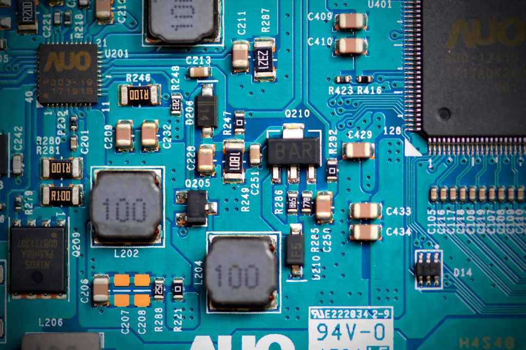
Via, Anti-Pad and High-Speed Connector Optimization
Vias and connectors are the main impedance discontinuity points. This serdes pcb design guide provides specific optimization techniques. For detailed manufacturing guidelines, refer to PCB Manufacturing.
Via Optimization: Eliminate via stubs by backdrilling (mandatory for 25G+); optimize anti-pad size; for high-density 112G designs, blind/buried vias can reduce via count.
Connector Optimization: Follow vendor official reference stackup strictly; keep complete ground reference under connector signal pins; only use 56G/112G certified high-speed backplane connectors for PAM4 applications.
PCB Material & Copper Foil Selection by SerDes Speed
Material grading is the foundation of SerDes performance. For detailed Dk/Df values, refer to High-Speed PCB Material.
- 25G / 28G NRZ: Standard low-loss FR4 is sufficient according to this serdes pcb design guide.
- 56G PAM4: Must upgrade to ultra-low-loss laminate with low Df value; Megtron series and Rogers materials are recommended.
- 112G PAM4: Require top-tier ultra-low-loss material plus HVLP low-profile copper foil.
For cost-sensitive projects, this serdes pcb design guide recommends hybrid stackup: apply ultra-low-loss material on high-speed SerDes layers, and standard low-loss material on ordinary signal layers.
Complete SerDes PCB Design Guide Layout Checklist
| ✅ | Item |
|---|---|
| ✅ | Confirm all differential pairs at 100Ω ±10% differential impedance |
| ✅ | Control intra-pair mismatch within 1–3mil; 112G PAM4 ≤1mil |
| ✅ | All 25G+ vias implemented with backdrilling |
| ✅ | Limit maximum 2 vias per SerDes lane |
| ✅ | Select matched low-loss or ultra-low-loss material per rate |
| ✅ | Complete channel insertion loss simulation |
| ✅ | No SerDes traces cross reference plane splits |
| ✅ | Adopt certified high-speed connectors and follow vendor guidelines |
Key Takeaways for SerDes PCB design guide
- SerDes rate upgrade must match material grade upgrade. This serdes pcb design guide emphasizes: 25G/28G for low-loss FR4, 56G/112G PAM4 for ultra-low-loss dielectric and HVLP copper foil.
- PAM4 design requires far stricter control than NRZ in impedance matching, length skew, and crosstalk suppression — a key insight from this serdes pcb design guide.
- Backdrilling is no longer optional — it becomes mandatory for all 25G and above SerDes layouts.
- Channel loss budget simulation must be done before layout; blind routing without simulation easily causes over-loss and link failure.
- Via anti-pad tuning, standardized connector routing and complete reference planes are indispensable for stable 25G–112G SerDes channel performance.
For a complete understanding of all high-speed interface layout requirements, return to the High-Speed Interfaces master page.
FAQ About SerDes PCB Design Guide
Q1: What is the standard differential impedance for SerDes routing?
100Ω differential impedance with ±10% tolerance is the universal standard for all 25G to 112G SerDes lanes. This serdes pcb design guide follows this standard throughout.
Q2: Is backdrilling required for 25G SerDes?
Yes. Backdrilling is mandatory for all 25G and higher SerDes to eliminate via stub resonance, as emphasized in this serdes pcb design guide.
Q3: What is the difference between NRZ and PAM4 in PCB design?
PAM4 has 4-level modulation with three narrow eye openings, lower SNR tolerance, stricter loss budget, higher requirement for material and copper foil roughness — a critical distinction in any serdes pcb design guide.
Q4: How much intra-pair length mismatch is allowed for 112G PAM4?
Strictly controlled within 1mil to minimize timing skew and eye margin loss, as specified in this serdes pcb design guide.
Q5: Can regular FR4 material be used for 56G PAM4 design?
No. Standard FR4 cannot meet high-frequency Df loss requirements; 56G PAM4 must use ultra-low-loss high-frequency laminates according to this serdes pcb design guide.
Professional SerDes PCB Design Guide Support & Quote
Designing reliable 25G, 56G and 112G NRZ/PAM4 SerDes PCB channels involves stackup optimization, impedance simulation, loss budget analysis, via tuning, backdrilling DFM, material selection and full signal integrity verification. This serdes pcb design guide provides the foundational rules, but real projects often require expert assistance.
Submit your project specifications now to get free technical review and competitive quotation for your high-speed SerDes PCB requirements.
© 2026 HighSpeedPCBs