How Via Stub and Anti Pad Design Affect Crosstalk in High Speed PCB
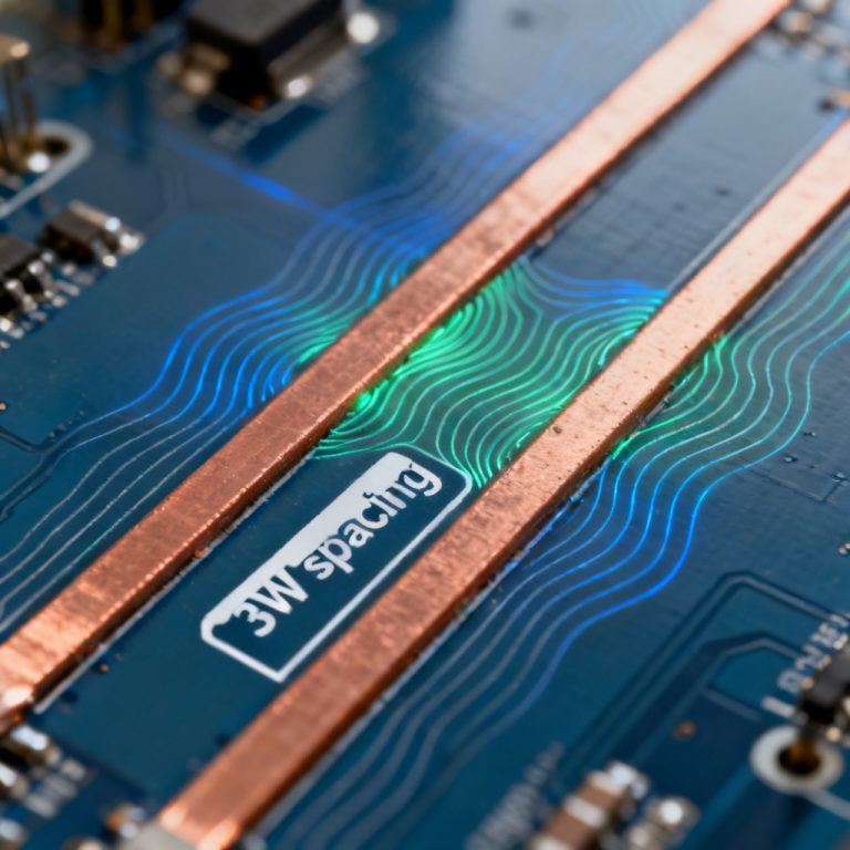
Understanding how via stub and anti-pad design affect crosstalk in high speed PCB is critical for modern signal integrity engineering. As data rates exceed 10 Gbps, the physical structure of vias—especially the unused barrel (stub) and the clearance hole (anti-pad)—becomes a dominant source of unwanted coupling. This pillar content explores the physics, resonance effects, and…