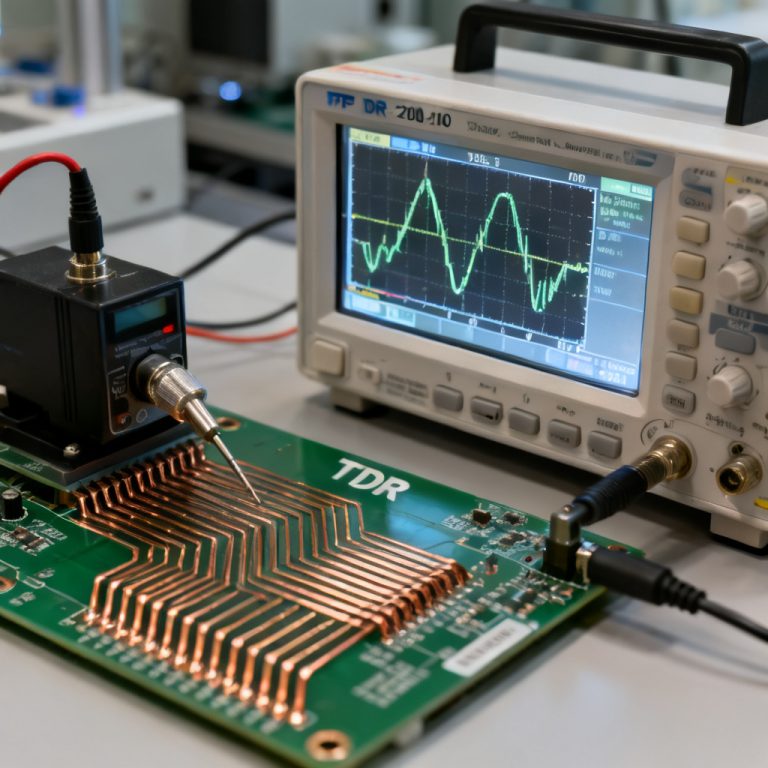
Understanding how via stub and anti-pad design affect crosstalk in high speed PCB is critical for modern signal integrity engineering. As data rates exceed 10 Gbps, the physical structure of vias—especially the unused barrel (stub) and the clearance hole (anti-pad)—becomes a dominant source of unwanted coupling. This pillar content explores the physics, resonance effects, and proven mitigation strategies to ensure reliable high-speed performance.
What Is a Via Stub and Why Does It Matter for Crosstalk in High Speed PCB?
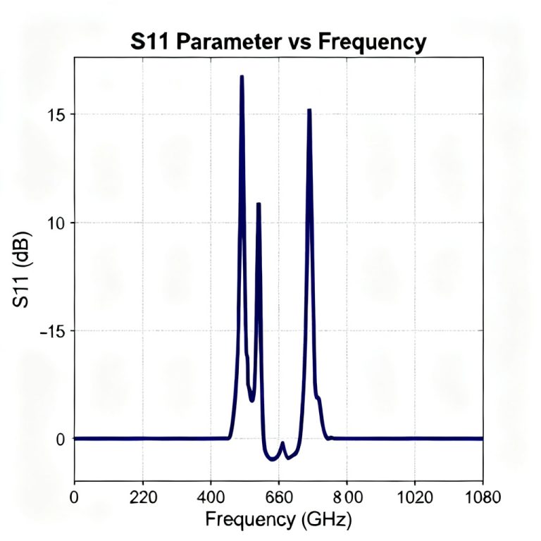
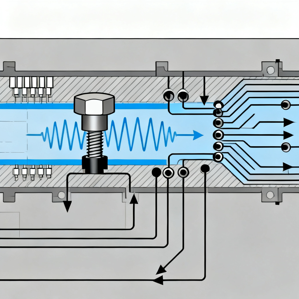
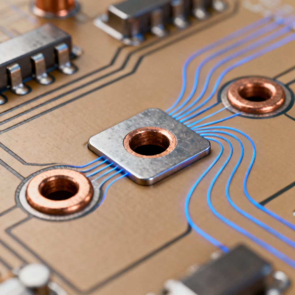
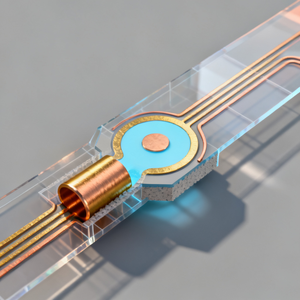
A via stub is the unused portion of a via barrel that extends beyond the target signal layer. In a high speed PCB, this stub acts as a quarter-wave resonator. At its resonant frequency, the stub reflects signal energy back to the source, creating a deep notch in insertion loss (S21). More critically, the stub couples energy into adjacent vias, directly increasing crosstalk in high speed PCB designs.
The resonance frequency is calculated as: F_res = c / (4 * L * √ε_r), where L is stub length and ε_r is dielectric constant. For a 100 mil stub in FR4 (ε_r ≈ 4), resonance occurs near 7.5 GHz. This makes stub management essential for any channel operating above 5 GHz.
How Stubs Create Crosstalk Mechanisms in High Speed PCB
There are three primary crosstalk mechanisms driven by via stubs:
- Shared stub resonance: When two signals share a common stub, energy from the aggressor resonates and couples into the victim via common impedance.
- Stub-to-stub coupling: Electromagnetic fields from a resonating stub capacitively and inductively couple into nearby stubs, especially in dense via arrays.
- Return path disruption: The stub creates an impedance discontinuity, forcing return current through longer paths that radiate and couple into adjacent structures.
Each of these mechanisms directly degrades crosstalk in high speed PCB performance, requiring deliberate mitigation.
Mitigation Strategies for Via Stubs
| Mitigation Technique | Effect on Crosstalk in High Speed PCB | Cost Impact |
|---|---|---|
| Back-drilling (controlled depth drilling) | Eliminates stub resonance, reducing crosstalk by >90% | Moderate |
| Blind/buried vias | Inherently eliminates stubs, best for 25+ Gbps | High |
| Stub termination (capacitor/resistor) | Shifts resonance frequency, reduces peak crosstalk | Low |
| Layer stack-up optimization | Minimizes stub length by routing signals near top/bottom | None |
Back-drilling is the most widely adopted solution for production high speed PCB designs, as it removes the stub without increasing layer count.
Anti-Pad Design: Controlling Impedance and Crosstalk in High Speed PCB
What Is an Anti-Pad and How Does It Affect Crosstalk in High Speed PCB?
The anti-pad is the clearance hole etched in power or ground planes around a via. Its diameter directly controls via impedance. A larger anti-pad increases impedance by reducing capacitance; a smaller anti-pad lowers impedance. For a 50Ω target, the anti-pad must be precisely sized using field solvers.
Regarding crosstalk in high speed PCB, the anti-pad acts as an aperture for fringing fields. A larger anti-pad, while good for impedance matching, increases capacitive coupling to adjacent vias. This trade-off must be carefully balanced.
Anti-Pad Coupling Mechanisms
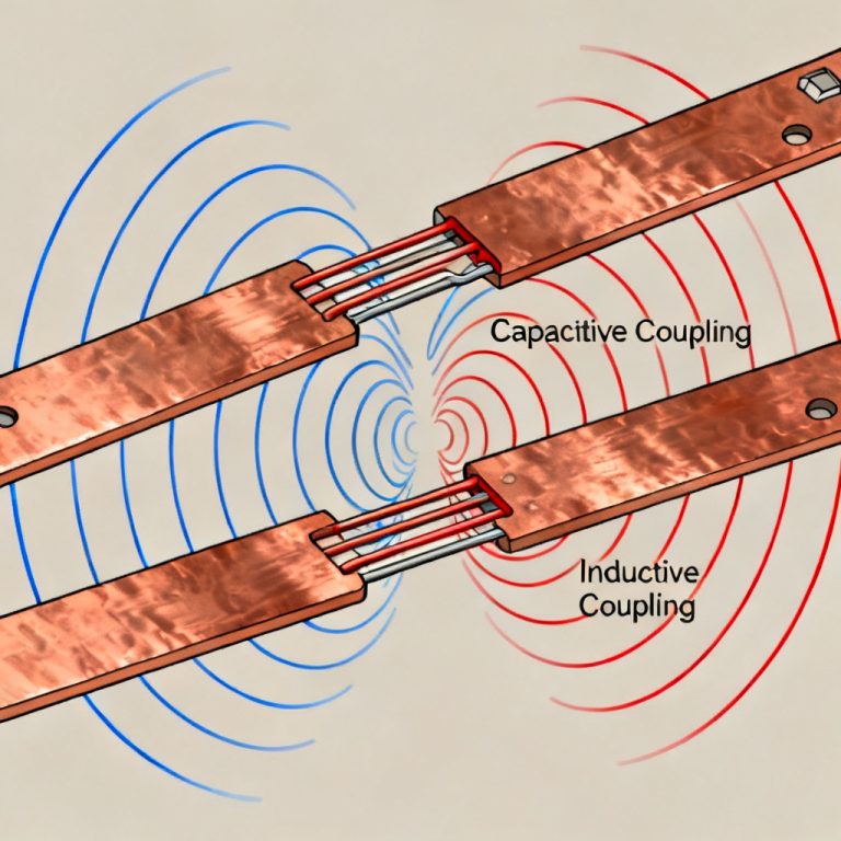
- Capacitive coupling: The fringing electric field from the aggressor via couples through the dielectric in the anti-pad void to the victim via.
- Inductive coupling: Magnetic fields from the current loop couple via mutual inductance, influenced by anti-pad size.
- Shared anti-pad coupling: When two vias share the same clearance hole, coupling becomes extremely strong—this must be avoided.
Proper anti-pad design is therefore a critical lever for managing crosstalk in high speed PCB.
Anti-Pad Design Best Practices for Reduced Crosstalk
| Design Practice | Impact on Crosstalk in High Speed PCB | Implementation Note |
|---|---|---|
| Optimized anti-pad diameter (field solver) | Matches impedance while minimizing coupling aperture | Use 2D/3D EM simulation |
| Non-circular (oval/slot) anti-pads for differential pairs | Equalizes coupling, improves odd-mode impedance | Common in 25+ Gbps designs |
| Ground via fencing (stitching vias) | Shields fringing fields, reduces crosstalk by 60-80% | Spacing < λ/20 at highest frequency |
| Avoid shared anti-pads | Prevents direct low-impedance coupling path | Minimum 5-10 mil copper web between anti-pads |
Ground via fencing is particularly effective: placing ground vias around signal vias provides a low-impedance return path and shields the fringing fields that cause crosstalk.
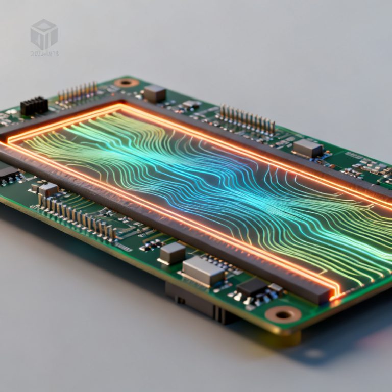
The Combined Effect: How Via Stubs and Anti-Pads Amplify Crosstalk in High Speed PCB
The most critical insight is that stubs and anti-pads act synergistically. A via stub creates a resonant structure; the anti-pad acts as the aperture through which resonant energy couples to adjacent vias. A poorly designed anti-pad (too large, shared) provides a large aperture for the stub’s resonant energy, dramatically amplifying crosstalk in high speed PCB at the resonant frequency.
Additionally, an impedance mismatch from an improperly sized anti-pad excites the stub resonance more efficiently. The combination of a long stub and a mismatched anti-pad creates a “perfect storm” for signal degradation and crosstalk.
At low frequencies, the anti-pad dominates crosstalk via capacitive coupling. At high frequencies (near stub resonance), the stub becomes the dominant factor. A comprehensive design must address both.
Best Practices for Minimizing Crosstalk in High Speed PCB
Design Rules Summary
- Eliminate stubs on critical nets: Use back-drilling for signals above 1 GHz; use blind/buried vias for 25-50 Gbps channels.
- Design anti-pads for 50Ω: Use field solvers; consider elongated anti-pads for differential pairs.
- Ground via fencing: Surround signal vias with ground vias; one ground via per 3-4 signal vias in a row; spacing 30-40 mil center-to-center.
- Never share anti-pads: Maintain at least 5-10 mil copper web between signal via anti-pads.
- Simulate, don’t guess: Use 3D EM solvers (HFSS, CST, EMPro) for channels above 5 GHz.
Following these rules ensures robust crosstalk in high speed PCB performance across the entire operating bandwidth.
Frequently Asked Questions About Via Stub and Anti-Pad Design for Crosstalk in High Speed PCB
What is the primary cause of crosstalk in high speed PCB vias?
The primary cause is the combination of via stub resonance and improper anti-pad design. The stub acts as a resonant antenna, while the anti-pad determines the coupling aperture. Together, they create a frequency-dependent crosstalk mechanism that degrades signal integrity.
How does back-drilling reduce crosstalk in high speed PCB?
Back-drilling removes the unused via stub, eliminating the quarter-wave resonance that amplifies crosstalk. This reduces the stub length to near zero, preventing the resonant coupling that occurs at specific frequencies.
Can anti-pad size affect crosstalk in high speed PCB?
Yes. A larger anti-pad increases capacitive coupling between adjacent vias because it creates a larger area for fringing electric fields. However, a smaller anti-pad lowers via impedance, causing reflections. The optimal anti-pad size balances impedance matching with minimal coupling.
What is the role of ground vias in reducing crosstalk in high speed PCB?
Ground vias provide a low-impedance return path and shield the electromagnetic fields from signal vias. When placed strategically around signal vias (via fencing), they can reduce crosstalk by 60-80% by containing the fringing fields within the ground via ring.
What is the recommended anti-pad diameter for a 50Ω high speed PCB via?
There is no universal value—it depends on stack-up, dielectric constant, and via pad size. A common starting point is an anti-pad 8-10 mils larger than the via pad on each side, but field solver simulation is strongly recommended for accurate impedance matching.
Comparison: Via Design Approaches for Crosstalk in High Speed PCB
| Design Approach | Crosstalk Reduction | Cost | Complexity | Best For |
|---|---|---|---|---|
| Standard through-hole via (no mitigation) | Baseline (poor) | Lowest | Lowest | Low-speed, <1 Gbps |
| Back-drilled via | Excellent (90%+ reduction) | Moderate | Moderate | 1-25 Gbps |
| Blind/buried via | Excellent (100% stub elimination) | High | High | 25+ Gbps, BGA fanout |
| Via with optimized anti-pad + ground fencing | Very good (60-80% reduction) | Low | Low | Up to 10 Gbps |
| Full 3D EM simulated via (stub + anti-pad optimized) | Best (near-ideal) | Moderate (simulation cost) | High | 25+ Gbps, critical channels |
Our high speed PCB fabrication services specialize in back-drilling, controlled impedance, and advanced via structures. We provide free 3D EM simulation support for critical channels to ensure optimal crosstalk performance.
Glossary of Key Terms for Crosstalk in High Speed PCB
- Via stub: The unused portion of a via barrel that extends beyond the signal layer, acting as a resonant antenna.
- Anti-pad: The clearance hole in a copper plane around a via, controlling impedance and coupling.
- Crosstalk: Unwanted coupling of energy from one signal to another, degrading signal integrity.
- Quarter-wave resonance: The frequency at which a via stub length equals one-quarter of the signal wavelength, causing maximum reflection.
- Back-drilling: A manufacturing process that removes the via stub after plating.
- Ground via fencing: Placement of ground vias around signal vias to shield electromagnetic fields.
- Impedance discontinuity: A change in characteristic impedance that causes signal reflections.
- Insertion loss (S21): The loss of signal power as it travels through a channel.