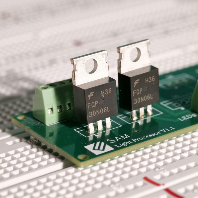
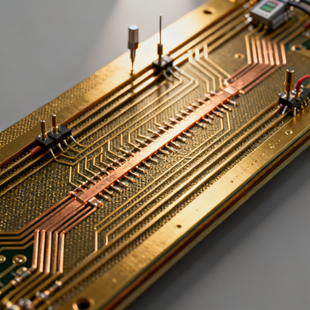
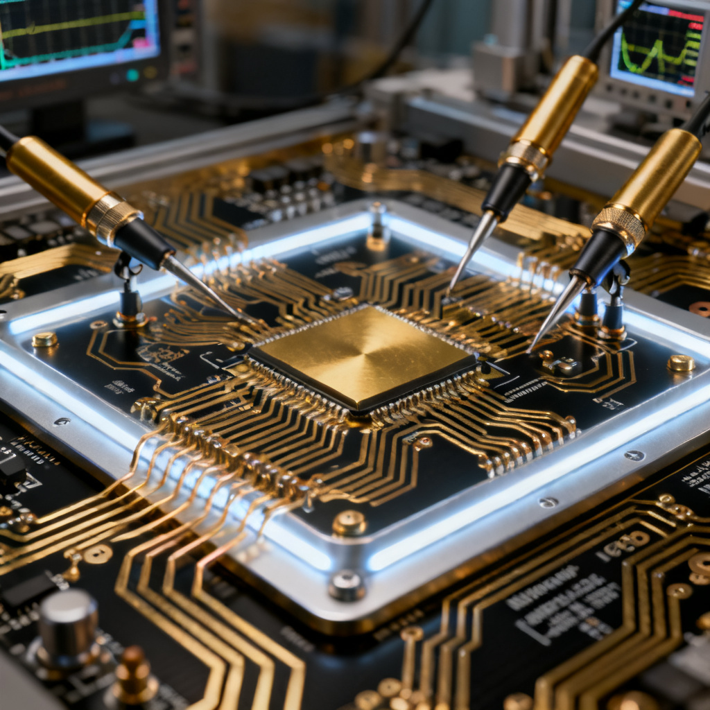
High Speed PCB design is a critical bottleneck for product success in 5G, AI, and high-frequency computing. Mastering High Speed PCB design ensures signal integrity and reliability at data rates exceeding 10 Gbps.
This pillar content synthesizes the top 10 challenges in High Speed PCB design, offering proven solutions from leading industry sources. Whether designing a 28-layer backplane or a compact RF module, these insights will help you achieve first-pass success.
Challenge 1: Signal Integrity in High Speed PCB Design
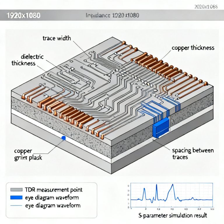
Reflections and Impedance Mismatch in High Speed PCB
At high frequencies above 100 MHz, any impedance discontinuity causes signal reflections, leading to ringing and data eye closure. In High Speed PCB systems like DDR4/5 or PCIe Gen 4/5, even a 10% impedance mismatch can degrade bit error rates significantly.
To overcome this in your High Speed PCB design, use controlled impedance with a field solver like Polar SI9000. For microstrip, keep trace width-to-height ratio above 2:1; for stripline, ensure symmetric stackup. Back-drilling removes unused via stubs, limiting stub length to under 10 mils for 25 Gbps signals. Apply series termination for point-to-point lines and parallel termination for multi-drop buses. For differential pairs, use 100Ω termination resistors. Match trace lengths within ±5 ps for parallel buses like DDR4.
Your PCB fabricator must provide impedance test coupons with a tolerance of ±10% or ±7% for critical designs. We offer certified impedance control with TDR testing for every panel.
Challenge 2: Crosstalk in High Speed PCB Layout
Near-End and Far-End Crosstalk in High Speed PCB
Aggressive trace spacing in dense High Speed PCB designs leads to electromagnetic coupling. Near-end crosstalk appears on the same layer; far-end crosstalk appears on adjacent layers, causing jitter and false triggering in serial links like USB 3.2.
For your High Speed PCB layout, follow the 3W rule for microstrip and 5W for stripline. Place grounded guard traces between aggressor and victim lines with vias spaced every λ/20. Route high-speed signals on stripline layers to reduce radiated crosstalk. Keep differential pairs tightly coupled and never split a pair across different layers without a via. Use simulation tools like HyperLynx to model crosstalk before fabrication.
Challenge 3: Power Integrity in High Speed PCB
Decoupling and PDN for High Speed PCB
High-speed switching creates transient current demands in your High Speed PCB. If the power distribution network has high impedance, voltage droops and ripple occur, causing logic errors.
To ensure power integrity in your High Speed PCB, use a solid ground plane and multiple power layers. Keep plane impedance below 10 mΩ up to 100 MHz. Place 0.1 μF and 0.01 μF decoupling capacitors close to each power pin. Use multiple parallel vias to reduce ESL. Avoid power plane resonances by adjusting plane dimensions and using a 3D EM solver.
Challenge 4: EMI in High Speed PCB Design
Electromagnetic Interference and Radiation in High Speed PCB
High-speed edges generate harmonic content up to the 10th harmonic in High Speed PCB designs. Unshielded traces and poor grounding cause radiated emissions that fail FCC testing.
To control EMI in your High Speed PCB, use metal shield cans over noisy ICs with low-impedance vias every 2 mm. Never route a high-speed trace over a split ground plane. Add ferrite beads on power inputs and common-mode chokes on differential pairs. Keep high-speed traces away from board edges and use 45° bends.
Challenge 5: Via Stubs in High Speed PCB
Via Optimization for High Speed PCB
In multi-layer High Speed PCB boards, through-hole vias create stubs that act as capacitive loads. At 10 Gbps, a 50-mil stub can cause 3 dB insertion loss.
To optimize vias in your High Speed PCB, specify back-drilling to remove unused stubs, limiting stub to under 10 mils. Use blind or buried micro-vias for high-density interconnects. Place multiple ground vias around signal vias to reduce inductance. Simulate via transitions using 3D EM tools.
Challenge 6: Dielectric Material Selection for High Speed PCB
Low-Loss Materials in High Speed PCB
Standard FR4 has high dielectric loss above 1 GHz in High Speed PCB applications. At 10 GHz, dielectric loss can reach 1 dB/inch.
For your High Speed PCB, use low-loss materials like Rogers 4350B, Megtron 6, or Isola Tachyon. Choose materials with tight Dk tolerance for consistent impedance. Use ENIG or immersion silver surface finish. Select low-loss prepreg near high-speed layers.
Challenge 7: Thermal Management in High Speed PCB
Heat Dissipation for High Speed PCB
High-speed processors in High Speed PCB designs dissipate 50-200W, causing thermal expansion mismatch and solder joint failure.
To manage heat in your High Speed PCB, use arrays of thermal vias under hot components. Use solid copper planes as heat spreaders and consider copper coins for direct heat sinking. Use high-Tg FR4 or polyimide for high-temperature environments.
Challenge 8: Skew in High Speed PCB Routing
Differential Pair and Clock Skew in High Speed PCB
In differential pairs, intra-pair skew causes common-mode conversion in High Speed PCB designs. In clock distribution, inter-pair skew violates setup times.
To minimize skew in your High Speed PCB, match P and N traces to within ±1 ps. Route both traces on the same layer and use a H-tree topology for clock distribution. Use low-skew buffers and programmable delay lines for fine adjustment.
Challenge 9: Return Path Discontinuities in High Speed PCB
Ground Plane Integrity for High Speed PCB
High-speed signals require a continuous return path in High Speed PCB designs. A gap in the ground plane creates inductance and common-mode noise.
To avoid return path issues in your High Speed PCB, never split ground planes under high-speed traces. Place stitching vias near signal vias when changing layers. Keep the same reference plane for the entire signal path. Use small antipads on ground layers.
Challenge 10: Simulation in High Speed PCB Design
Verification Complexity in High Speed PCB
High-speed PCB design without simulation is risky in High Speed PCB projects. Post-layout verification is expensive and time-consuming.
To overcome this in your High Speed PCB design, use pre-layout simulation tools like HyperLynx for channel simulation. Use SI-aware design rules from your PCB CAD tool. Order a small batch for validation before mass production. Choose a manufacturer that offers SI/PI simulation services.
High Speed PCB Design Specifications Table
| Parameter | High Speed PCB Specification |
|---|---|
| Impedance Tolerance | ±7% for critical High Speed PCB designs |
| Max Via Stub Length | 10 mils for 25 Gbps High Speed PCB |
| Dielectric Loss (Df) | Below 0.005 for High Speed PCB above 5 Gbps |
| Thermal Via Pitch | 0.5 mm for High Speed PCB heat dissipation |
Comparison: Standard vs. High Speed PCB Design
Standard PCB design uses FR4 with 10% impedance tolerance, while High Speed PCB design requires low-loss materials with ±7% tolerance. Standard design ignores via stub effects, but High Speed PCB design mandates back-drilling. Standard layout uses 2W spacing, but High Speed PCB layout requires 3W or 5W spacing for crosstalk control. Our manufacturing process supports all High Speed PCB requirements with certified impedance control and advanced materials.
Glossary of High Speed PCB Terms
Signal Integrity (SI): The quality of electrical signals in High Speed PCB designs, measured by eye diagram and bit error rate.
Crosstalk: Electromagnetic coupling between traces in High Speed PCB layouts.
Power Integrity (PI): Stability of power distribution in High Speed PCB systems.
Back-Drilling: A process to remove via stubs in High Speed PCB fabrication.
Dielectric Loss (Df): Energy dissipation in High Speed PCB materials at high frequencies.
Frequently Asked Questions about High Speed PCB
What is the most critical factor in High Speed PCB design?
Signal integrity is the most critical factor in High Speed PCB design, requiring controlled impedance and proper termination.
How do I choose materials for High Speed PCB?
Select low-loss materials like Rogers 4350B for High Speed PCB designs above 5 Gbps to minimize dielectric loss.
Why is back-drilling important in High Speed PCB?
Back-drilling removes via stubs in High Speed PCB to reduce signal reflections and insertion loss at high frequencies.
How can I reduce crosstalk in High Speed PCB?
Use 3W spacing and guard traces in your High Speed PCB layout to minimize electromagnetic coupling.
What is the best stackup for High Speed PCB?
A 4-layer stackup (signal-ground-power-signal) is recommended for simple High Speed PCB designs, while 6+ layers are needed for complex ones.
Conclusion: Partner for High Speed PCB Success
By addressing these 10 challenges in High Speed PCB design, you can achieve reliable, high-performance products. We offer controlled impedance with ±7% tolerance, advanced materials like Rogers and Megtron, HDI capabilities including micro-vias and back-drilling, and free SI/PI simulation for qualified projects. Get a quote today with your Gerber files for a DFM review within 24 hours.