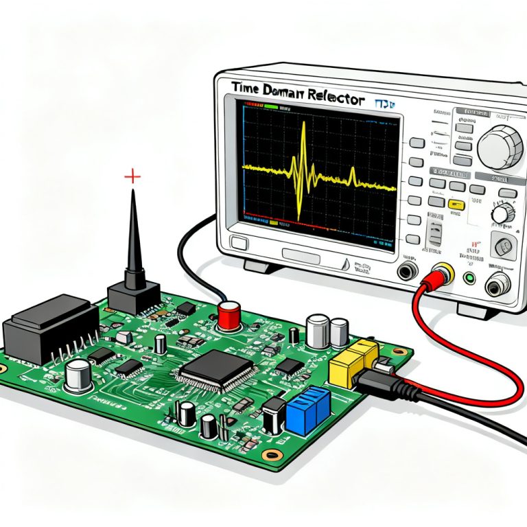
In high-speed PCB design, signal integrity depends on precise timing. A jitter report for high speed PCB design review reveals timing deviations that can break multi-gigabit links. This guide teaches you to generate, interpret, and act on a professional jitter report.
1. Understand the Jitter Report for High Speed PCB Design Review Fundamentals
Before generating a jitter report for high speed PCB design review, you must grasp core definitions. All top industry sources agree on this taxonomy:
- Total Jitter (TJ): Peak-to-peak jitter at a specific bit error rate (BER), typically 10⁻¹² for high-speed serial links. TJ = 14.069 × σRJ + DJ (for BER=10⁻¹²).
- Random Jitter (RJ): Gaussian, unbounded, caused by thermal noise, shot noise, flicker noise. Characterized by standard deviation (σ).
- Deterministic Jitter (DJ): Bounded and predictable, subdivided into:
- Periodic Jitter (PJ): From power supply noise, clock coupling, switching regulator ripple.
- Data-Dependent Jitter (DDJ)/ISI: From bandwidth limitations, impedance mismatches, reflections.
- Duty Cycle Distortion (DCD): From asymmetric rise/fall times or threshold offsets.
- Bounded Uncorrelated Jitter (BUJ): From crosstalk from neighboring aggressor signals.
Key insight: In a design review, separate RJ from DJ using a bathtub curve or BER contour. The report must show DJ breakdown to identify root causes.

2. Prepare Your Simulation for a Jitter Report for High Speed PCB Design Review
To generate a reliable jitter report for high speed PCB design review, follow these pre-simulation steps:
- Extract S-Parameters: Use a 3D field solver (e.g., Ansys HFSS, CST) to extract S-parameters of the entire channel—driver to receiver, including vias, connectors, PCB traces.
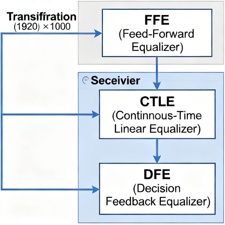
- Use IBIS-AMI Models: Accurate transmitter (Tx) and receiver (Rx) models including equalization (CTLE, DFE, FFE).
- Define Data Pattern: Use PRBS-7 (for 8b/10b encoded links) or PRBS-31 (for 64b/66b encoded links).
- Set BER Target: Most standards (PCIe, USB, Ethernet) require BER = 10⁻¹².
Pro tip: Always include power integrity (PI) in simulation. Jitter from PDN noise (PJ) can dominate the DJ budget if ignored.
2.1 Running the Time-Domain Simulation
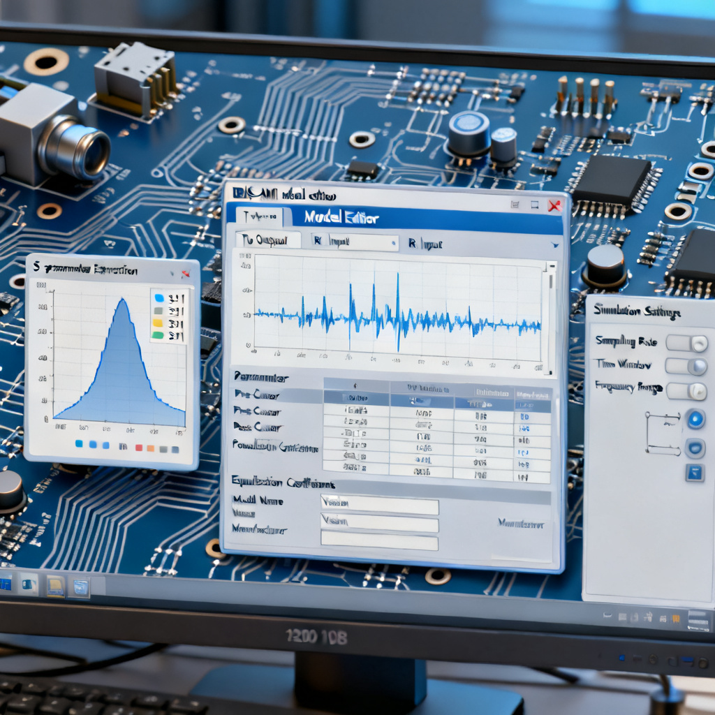
In your EDA tool (Altium, ADS, HyperLynx), configure a transient simulation over millions of bits. Simulate at least 1 million bits for accurate RJ estimation. Enable eye diagram and histogram collection. The horizontal eye opening (in ps) directly correlates to jitter. Collect zero-crossing times of each rising and falling edge—this raw data builds the jitter histogram.
2.2 Decompose Jitter Using the Dual-Dirac Model
Both industry standards agree on the Dual-Dirac Model for decomposition:
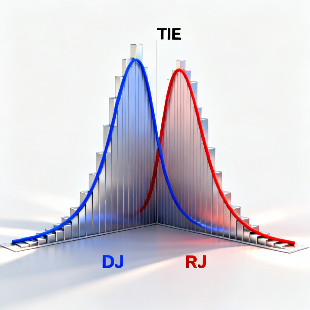
- Build the TIE (Time Interval Error) Histogram: TIE measures the difference between actual edge timing and ideal clock edge.
- Separate Left and Right Histograms: Fit two Gaussian curves to the left and right tails. The distance between means = Deterministic Jitter (DJ). The standard deviation = Random Jitter (RJ).
- Calculate Total Jitter (TJ): TJ(10⁻¹²) = 14.069 × σRJ + DJ.
Warning: Do not read peak-to-peak jitter from the histogram alone. That value is unbounded. Always use the Dual-Dirac method with a defined BER.
2.3 Isolate DJ Components
To fix jitter, identify its source. The report must include a Jitter Breakdown section:
- Identifying Periodic Jitter (PJ): Use a phase noise plot or FFT of the TIE data. A spike at a specific frequency (e.g., 100 MHz switching noise) indicates PJ.
- Identifying ISI (DDJ): Use a Pattern-Dependent Jitter analysis. Plot jitter versus data pattern. High jitter after long runs of 1s or 0s indicates ISI.
- Identifying DCD: Check the Duty Cycle of the eye diagram. If crossing point is not at 50%, DCD is present.
3. Interpret the Jitter Report for High Speed PCB Design Review
A jitter report for high speed PCB design review is useless without context. Answer three questions:
- Does the design meet the jitter budget? Compare TJ against the standard’s specification (e.g., PCIe Gen 4 requires < 0.3 UI pk-pk jitter at BER 10⁻¹²).
- What is the dominant jitter component?
- RJ dominates: Issue in PLL, power supply, or substrate noise. Action: Improve power filtering, use LDOs near the clock.
- ISI (DDJ) dominates: Channel is lossy. Action: Reduce trace length, use lower-loss materials (e.g., Megtron 6 vs. FR-4), optimize via stub length, improve equalization.
- PJ dominates: Coupling issue. Action: Check isolation between clock and high-speed data lines; add ferrite beads or decoupling caps.
- Where is the worst-case jitter occurring? Create a jitter heat map on the PCB layout. Highlight areas where jitter exceeds 50% of the budget.
4. Present the Final Jitter Report for High Speed PCB Design Review
Your final jitter report for high speed PCB design review should be a structured document including:
- Executive Summary: Pass/Fail status against the standard.
- Measurement Setup: Software version, model files used, BER target.
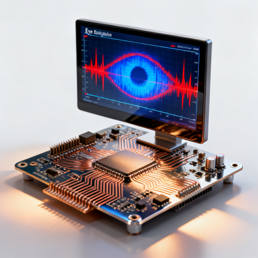
- Eye Diagram: With horizontal and vertical eye opening measurements.
- Bathtub Curve: Showing BER vs. timing margin. Must show a clear “bathtub” shape.
- Jitter Decomposition Table:
| Jitter Component | Value (ps) |
|---|---|
| Total Jitter (TJ) at BER 10⁻¹² | X ps |
| Random Jitter (RJ) σ | X ps |
| Deterministic Jitter (DJ) | X ps |
| Periodic Jitter (PJ) | X ps |
| Data-Dependent Jitter (DDJ/ISI) | X ps |
| Duty Cycle Distortion (DCD) | X ps |
- Root Cause Analysis: A paragraph explaining the primary contributor and recommended design changes (e.g., “Increase trace width by 10% to reduce skin effect loss, or add a CTLE boost of +3 dB”).
FAQ: Jitter Report for High Speed PCB Design Review
What is a jitter report for high speed PCB design review?
A jitter report for high speed PCB design review is a detailed analysis of timing deviations in high-speed signals, decomposed into random and deterministic components, used to validate signal integrity against industry standards.
How do I generate a jitter report for high speed PCB design review?
Use EDA tools like Altium, Cadence Sigrity, or ADS. Extract S-parameters, run transient simulation with PRBS patterns, apply the Dual-Dirac model to decompose jitter, and present results in a structured report with eye diagrams and bathtub curves.
Why is a jitter report important for high speed PCB design review?
It identifies root causes of timing errors—such as ISI, PJ, or RJ—enabling targeted design fixes to meet BER requirements for standards like PCIe, USB, and Ethernet.
What is the Dual-Dirac model in a jitter report?
The Dual-Dirac model fits two Gaussian curves to the left and right tails of the TIE histogram. The distance between means gives Deterministic Jitter (DJ); the standard deviation gives Random Jitter (RJ). This is the industry-standard method for calculating Total Jitter at a specific BER.
How can I reduce jitter in my high-speed PCB design?
Based on the jitter report for high speed PCB design review: for RJ, improve power filtering and PLL design; for ISI, use lower-loss materials and optimize via stubs; for PJ, isolate clock lines and add decoupling capacitors.
Conclusion: Use the Jitter Report as a Design Tool
A well-generated jitter report for high speed PCB design review is not just a compliance checkbox—it is a diagnostic tool that guides high-speed PCB design. By combining the Dual-Dirac model, isolating DJ components via FFT, and interpreting the bathtub curve, you can transform a noisy prototype into a robust, production-ready design.
Next Steps for Your Design Review:
- Download the simulation script from your EDA vendor.
- Set up a standard PRBS-31 pattern.
- Run the jitter decomposition.
- If TJ exceeds the budget, revisit the stack-up and routing.
At [Your Company Name], we specialize in manufacturing high-speed PCBs with controlled impedance and low-loss materials. Contact us for a free design for manufacturing (DFM) review to ensure your jitter budget is met in production.