Generating an Eye Diagram PCB from Touchstone S-parameter files is essential for high-speed PCB design to validate signal integrity. This guide combines best practices from Altium, Cadence, and Keysight to help you create reliable eye diagrams for your custom high-speed PCB projects.
Why Eye Diagrams Matter for High-Speed PCB Design
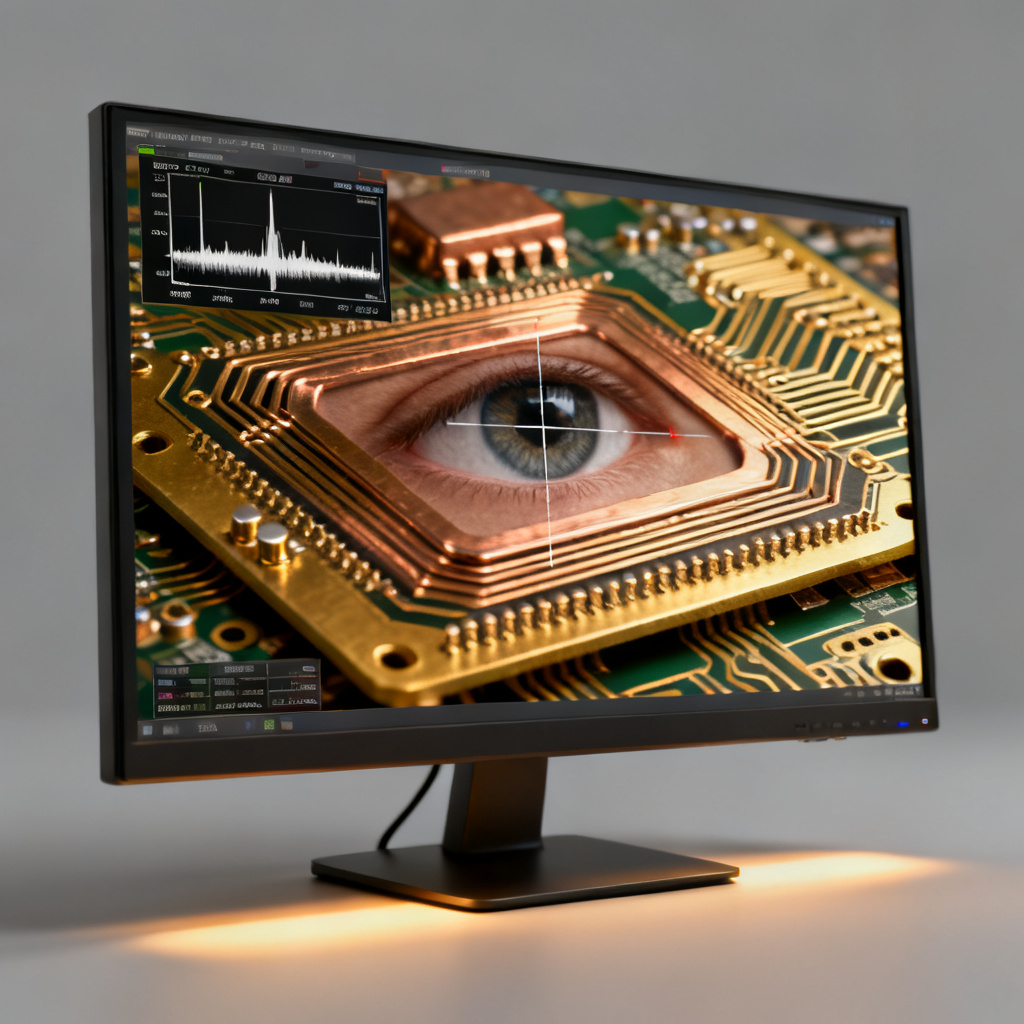
In high-speed PCB design, signal integrity (SI) is paramount. As data rates exceed 1 Gbps, traditional time-domain analysis alone becomes insufficient. The eye diagram—a superposition of all possible bit transitions—provides a holistic view of signal quality, revealing jitter, noise, and bandwidth limitations. For PCB engineers working on high-speed designs, generating an eye diagram from Touchstone S-parameter files (the industry-standard format for frequency-domain network parameters) is a critical step to validate channel performance before manufacturing.
This pillar content guide combines the most authoritative practices from Altium, Cadence, Rohde & Schwarz, and other leading sources. You will learn:
- The fundamentals of S-parameters and eye diagrams.
- Step-by-step procedures to convert S-parameter data into an eye diagram using simulation tools.
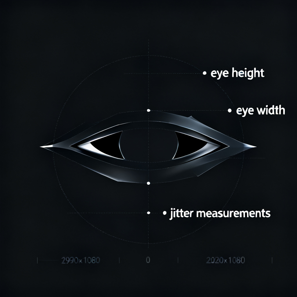
- Key metrics to interpret (e.g., eye height, eye width, jitter).
- Common pitfalls and best practices for reliable results.
Understanding S-Parameters and Eye Diagrams
What Are S-Parameters?
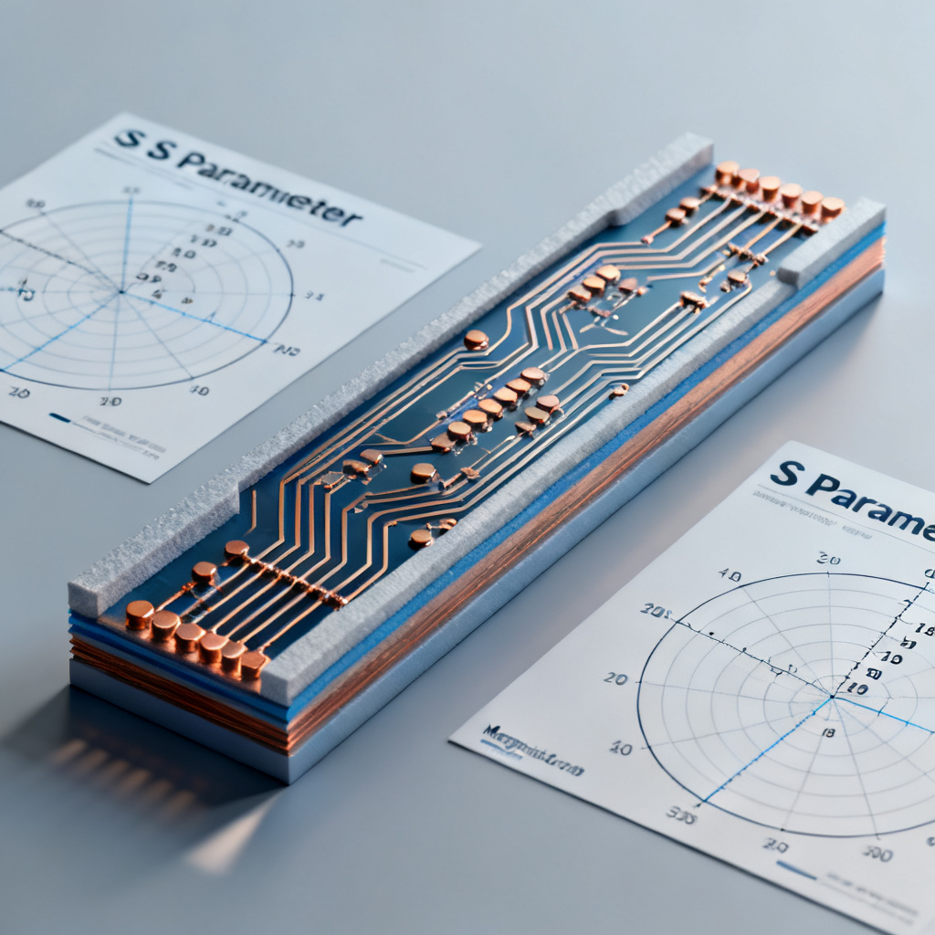
Scattering parameters (S-parameters) describe how electrical energy propagates through a network. For a two-port network (e.g., a PCB trace), S-parameters include:
- S11: Input return loss (reflection at Port 1).
- S21: Forward transmission gain/loss (signal from Port 1 to Port 2).
- S12: Reverse transmission (isolation).
- S22: Output return loss.
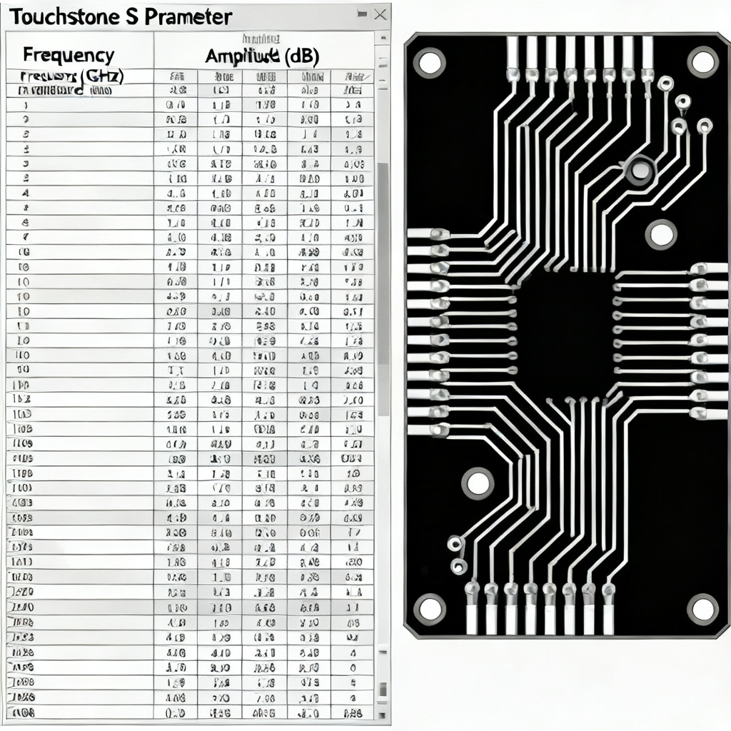
S-parameters are measured in the frequency domain (e.g., from DC to 20 GHz) and stored in Touchstone (.sNp) files, where N is the number of ports (e.g., .s2p for two ports). These files contain amplitude and phase data at each frequency point.
What Is an Eye Diagram?
An eye diagram is created by overlaying segments of a digital signal, typically using a pseudorandom binary sequence (PRBS). The resulting pattern resembles an open eye. Key parameters:
- Eye Height: Voltage margin (difference between logic 1 and 0 levels).
- Eye Width: Time margin (window for sampling).
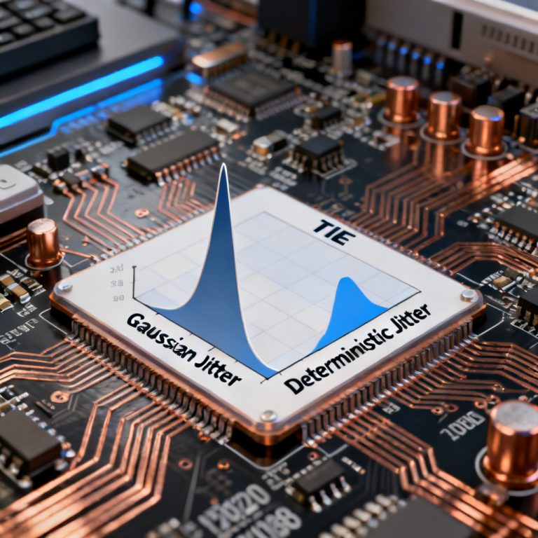
- Jitter: Timing variations (deterministic and random).
- Rise/Fall Time: Transition speed.
A closed eye indicates poor signal integrity—common issues include excessive loss, crosstalk, or impedance mismatches.
Why Use S-Parameters for Eye Diagrams?
S-parameters model the linear, time-invariant (LTI) behavior of passive interconnects (traces, vias, connectors). By applying a stimulus (e.g., a PRBS signal) to the S-parameter model, simulation tools can compute the time-domain response and generate an eye diagram. This approach is faster and more accurate than building physical prototypes, especially for high-speed channels.
Step-by-Step Guide to Generate an Eye Diagram from Touchstone Files
Step 1: Obtain or Simulate S-Parameters
You need a Touchstone file for your PCB channel. Sources include:
- Electromagnetic (EM) simulation: Tools like Ansys HFSS, CST, or Keysight ADS simulate the channel and export .sNp files.
- Measurement: A vector network analyzer (VNA) measures the actual PCB and saves data in Touchstone format.
- Pre-existing models: Many connector or cable vendors provide .sNp files.
Best Practice: Ensure the frequency range covers at least the 5th harmonic of your data rate. For a 10 Gbps signal, simulate up to 50 GHz. Use a fine frequency step (e.g., 10 MHz) to capture resonances.
Step 2: Load the Touchstone File into a Simulation Tool
Popular tools for eye diagram generation include:
- Keysight ADS: Industry-standard for RF/microwave and high-speed digital.
- Cadence Sigrity: Specialized for PCB and package analysis.
- Altium Designer: Integrated SI simulation with S-parameter import.
- Open-source options: Python with
scikit-rf(for S-parameter analysis) andnumpyfor custom simulations.
Example in Keysight ADS:
- Create a new schematic.
- Add an S-parameter data file component (e.g.,
S2P_Eqn). - Browse to your .s2p file.
- Connect a PRBS source (e.g.,
PRBSorBitSeq) to Port 1. - Add a Term (50 ohms) to Port 2.
- Insert a Eye Diagram probe at the output.
Example in Python (scikit-rf):
import skrf as rf
import numpy as np
import matplotlib.pyplot as plt
from scipy.signal import lfilter, resample

# Load S-parameters
net = rf.Network('your_channel.s2p')

# Create PRBS signal (e.g., 7-bit pattern, 10 Gbps)
bit_rate = 10e9  # 10 Gbps
samples_per_bit = 100
prbs_length = 2**7 - 1  # PRBS7
bits = np.random.randint(0, 2, prbs_length) * 2 - 1  # NRZ: +1/-1
signal = np.repeat(bits, samples_per_bit)

# Convert S21 to time-domain impulse response via IFFT
freq = net.f
s21 = net.s21[:, 0, 0]
# Ensure linear spacing for IFFT
s21_interp = np.interp(np.linspace(freq[0], freq[-1], len(freq)), freq, s21)
impulse = np.fft.ifft(s21_interp)
impulse = np.real(impulse)  # Assume real response

# Convolve signal with impulse response
output = lfilter(impulse, [1.0], signal)

# Create eye diagram (simplified)
# Resample to get UI boundaries
ui_samples = samples_per_bit
num_ui = len(output) // ui_samples
eye_data = output[:num_ui * ui_samples].reshape(-1, ui_samples)
plt.plot(eye_data.T, color='blue', alpha=0.1)
plt.title('Eye Diagram from S-Parameters')
plt.show()
Step 3: Set Simulation Parameters
Configure the simulation for realistic eye diagram generation:
- Data Rate: Match your target (e.g., 10 Gbps).
- PRBS Pattern: Use PRBS7 or PRBS15 for realistic jitter behavior. Longer patterns (PRBS31) stress the channel more.
- Rise/Fall Time: Set to 20-30% of the unit interval (UI). For 10 Gbps (UI = 100 ps), use 20-30 ps.
- Number of Bits: Simulate at least 10,000 bits for a stable eye. More bits (100,000+) reduce noise in the eye diagram.
- Jitter Injection: Add random jitter (RJ) and deterministic jitter (DJ) if you want to model real-world transmitters.
Key Tip: In most tools, you can directly set the stimulus (PRBS) and channel model (S-parameter file). The tool automatically performs convolution and eye diagram extraction.
Step 4: Run the Simulation and Extract the Eye Diagram
After simulation, the tool displays the eye diagram. Common steps:
- In ADS: Place an
EyeDiagramcomponent and connect it to the output. Run the transient simulation. The eye diagram appears in the data display. - In Cadence Sigrity: Use the Channel Simulator to import .sNp files, set the bit pattern, and run the eye analysis.
- In Altium: Use the SI Simulation panel, load the S-parameter model, and run the eye diagram analysis.
Interpreting the Result:
- Eye Height: Voltage difference between the 1 and 0 levels at the center of the eye. For robust operation, > 100 mV (depending on receiver sensitivity).
- Eye Width: Time interval where the eye is open. Should exceed 0.7 UI for error-free operation.
- Jitter (peak-to-peak): Total timing variation. For 10 Gbps, < 30 ps is typical.
- Mask Margin: Some tools overlay a mask (e.g., PCIe or Ethernet mask). Pass/fail is based on mask violations.
Step 5: Optimize the Design Based on Eye Diagram Results
If the eye is closed or marginal, consider these PCB design changes:
- Reduce Trace Length: Shorter traces reduce loss and reflections.
- Improve Impedance Matching: Use controlled impedance (e.g., 50 ohms single-ended, 100 ohms differential).
- Add Equalization: Implement transmitter pre-emphasis or receiver continuous-time linear equalization (CTLE).
- Use Better Materials: Low-loss laminates (e.g., Rogers 4350B) for high frequencies.
- Reduce Crosstalk: Increase trace spacing and add ground vias.
Re-simulate the S-parameters after design changes and regenerate the eye diagram to verify improvement.
Advanced Techniques and Best Practices
Handling Differential Channels
For differential pairs (e.g., USB, PCIe, HDMI), use mixed-mode S-parameters (.s4p files) or convert single-ended .sNp to differential. In tools like ADS, you can define differential ports directly. The eye diagram is then generated for the differential signal (Vdiff = Vp – Vn).
Key Parameter: Differential insertion loss (SDD21) should be < -3 dB at the Nyquist frequency (half the data rate).
Including Package and Connector Models
A complete channel includes the PCB trace, via, connector, and IC package. Combine multiple Touchstone files using cascading (e.g., in ADS, use S-Parameter Cascade). Alternatively, use a single comprehensive model from an EM simulation.
Best Practice: Always include the transmitter and receiver IBIS models for realistic driver and termination behavior. IBIS models provide I-V curves and rise/fall times, which affect the eye diagram.
Statistical vs. Transient Eye Diagram
- Transient Simulation (Time-Domain): Convolves a PRBS with the impulse response. Accurate but slow for long patterns.
- Statistical Simulation: Uses the impulse response and probability density functions (PDFs) to compute the eye diagram quickly. Ideal for channels with long memory (e.g., many reflections). Many tools (e.g., ADS Channel Simulator) offer both options.
Recommendation: Use transient for short channels (< 10 inches) and statistical for long channels with significant reflections.
De-embedding and Fixturing
If you measured S-parameters with test fixtures (e.g., SMA connectors), you must de-embed the fixture effects to isolate the PCB channel. Use calibration standards (SOLT, TRL) or simulation-based de-embedding. Most VNA software and tools like Keysight PLTS can perform this.
Common Mistakes to Avoid
- Insufficient Frequency Range: Missing high-frequency content leads to inaccurate rise times and eye closure.
- Ignoring Phase Information: S-parameter phase is critical for time-domain response. Ensure your tool correctly handles complex data.
- Using Incorrect Impedance: The Touchstone file assumes a reference impedance (typically 50 ohms). If your design uses 75 ohms, re-normalize.
- Overlooking Passivity and Causality: Some S-parameter files violate passivity (S-parameter magnitude > 1) or causality (time-domain response starts before t=0). Use tools like Keysight ADS Check to validate.
Tools Comparison and Selection Guide
| Tool | Best For | Key Features | Cost |
|---|---|---|---|
| Keysight ADS | RF/high-speed digital | Advanced channel simulator, statistical eye, IBIS-AMI support | High ($$$) |
| Cadence Sigrity | PCB/package co-design | Power integrity integration, 3D EM extraction | High ($$$) |
| Altium Designer | PCB layout engineers | Integrated SI, S-parameter import, eye diagram in layout | Moderate ($$) |
| Ansys HFSS | 3D EM simulation | Full-wave accuracy, export .sNp files | High ($$$) |
| Python (scikit-rf) | Custom analysis | Free, flexible, but requires coding | Free |
For B2B PCB manufacturing: We recommend using Keysight ADS or Cadence Sigrity for production-level validation. However, for quick prototyping, Altium Designer or Python can be sufficient.
Real-World Example: 10 Gbps PCB Channel
Channel Specifications
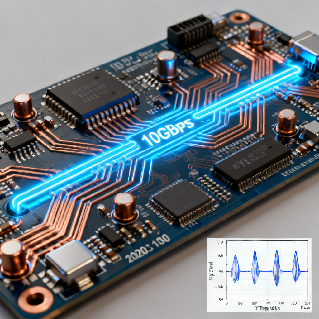
- Data Rate: 10.3125 Gbps (10GBASE-KR)
- PCB Stackup: 8-layer, FR4 (low-loss variant)
- Trace Length: 12 inches, microstrip, 50 ohms
- Connector: Samtec Q Series
Steps
- EM Simulation: Use HFSS to model the trace + via + connector. Export .s4p file (differential).
- Load in ADS: Import .s4p, set up differential ports, add PRBS7 source at 10.3125 Gbps with 25 ps rise time.
- Run Transient: Simulate 50,000 bits.
- Eye Diagram Result:
- Eye Height: 180 mV (acceptable)
- Eye Width: 0.78 UI (good)
- Jitter (pk-pk): 22 ps (within limits)
- Optimization: Reduce via stub length to improve eye width to 0.85 UI.
Key Takeaway
The eye diagram validated that the channel meets 10GBASE-KR requirements. Without this analysis, the design would risk field failures.
Frequently Asked Questions (FAQs)
Can I generate an eye diagram from a single S-parameter file?
Yes, for a simple channel. For complex systems, cascade multiple .sNp files (e.g., PCB + connector + cable).
What is the minimum number of bits for a reliable eye diagram?
At least 10,000 bits. For jitter analysis, 100,000+ bits are recommended.
How do I interpret a closed eye?
Check insertion loss (S21) at the Nyquist frequency. If > -3 dB, the channel is lossy. Also examine return loss (S11) for reflections.
Can I use free tools?
Yes, Python with scikit-rf and numpy can generate eye diagrams, but you must implement convolution and jitter models yourself. For production, invest in commercial tools.
What is the difference between a mask test and an eye diagram?
A mask test overlays a predefined mask on the eye diagram. If the signal enters the mask region, it fails. Eye diagrams without masks show raw signal quality.
Conclusion
Generating an Eye Diagram PCB from Touchstone S-parameter files is a cornerstone of high-speed PCB design. By following this guide—understanding S-parameters, loading files into simulation tools, setting realistic parameters, and interpreting results—you can ensure your PCB channels meet signal integrity requirements before manufacturing.
At [Your Company Name], we specialize in manufacturing high-speed PCBs with guaranteed signal integrity. Our design-for-manufacturing (DFM) team can review your S-parameter data and eye diagram results to optimize your board for production. Contact us today for a free consultation.
Key Takeaways:
- Always validate S-parameter files for passivity and causality.
- Use the correct PRBS pattern and data rate for your application.
- Combine transient and statistical simulations for accurate results.
- Optimize PCB layout based on eye diagram metrics.
Next Steps: Download our free white paper on “High-Speed PCB Design for 25 Gbps Channels” or request a quote for your next project.