Inter-Symbol Interference (ISI) is a critical signal integrity challenge in high-speed PCB design, directly impacting the reliability of data transmission. This pillar page explores the causes of ISI, how to detect it using eye diagrams, and provides actionable mitigation strategies for your high-speed PCB projects.
Causes of ISI in High-Speed PCB Design
Inter-Symbol Interference in high-speed PCB arises from several physical phenomena that distort the transmitted signal, causing one bit to interfere with subsequent bits.
Channel Bandwidth Limitations (Low-Pass Filter Effect)
Every PCB trace, via, and connector acts as a low-pass filter. High-frequency components (sharp edges of a digital signal) are attenuated more than low-frequency components. This smears the signal in time. For example, a single ‘1’ bit may not reach its full voltage swing, and its falling edge may drag into the next bit slot, making a following ‘0’ look like a ‘1’. This is the most common cause of ISI in high-speed serial links.
Impedance Discontinuities and Reflections
When a signal encounters an impedance mismatch (e.g., a change in trace width, a via stub, or a connector), part of the signal energy is reflected back toward the source. These reflections can arrive at the receiver delayed, superimposing on subsequent bits. A reflection from a previous bit can add to or subtract from the voltage of the current bit, causing data-dependent jitter and amplitude distortion.
Skin Effect and Dielectric Loss
At high frequencies, current flows only on the surface of the copper (skin effect), increasing resistance. Simultaneously, the PCB substrate (e.g., FR-4) absorbs energy (dielectric loss). Both effects are frequency-dependent. They cause different spectral components of the signal to travel at different speeds and with different attenuations. This dispersion spreads the pulse in time, creating a long tail that interferes with later bits.
Unintentional Crosstalk and Coupling
While often considered a separate issue, crosstalk from adjacent traces can introduce ISI-like behavior. If a strong transition on an aggressor line couples into a victim line, it can shift the zero-crossing point of the victim’s signal, adding to the timing jitter that degrades the eye diagram.
Detection of ISI Using Eye Diagrams
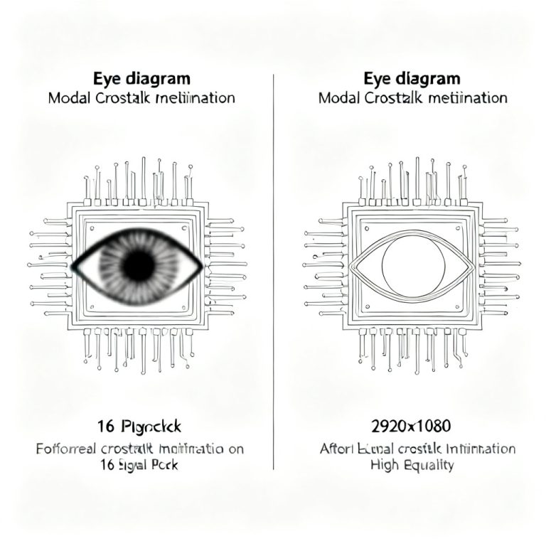
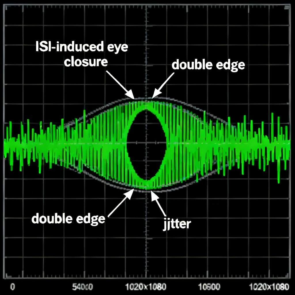
The eye diagram is the most powerful tool for visualizing ISI. It is created by overlaying many bit periods on an oscilloscope, triggered by the data clock. A healthy eye is wide open, with a clear center. ISI manifests in several telltale signs.
Key Eye Diagram Metrics Affected by ISI
Inter-Symbol Interference in high-speed PCB directly reduces eye height and eye width. Eye height (vertical opening) is the voltage margin between a logic ‘1’ and ‘0’. A closed eye height indicates that noise and distortion are eating into the signal. Eye width (horizontal opening) is reduced by deterministic jitter (DJ), which is data-dependent—long runs of identical bits (e.g., 00000) have different timing than a single isolated bit (e.g., 010).
How to Read ISI in an Eye Diagram
When you look at an eye diagram on a sampling oscilloscope or simulation tool, look for a “fuzzy” or “thick” eye, meaning multiple overlapping traces that show the signal’s trajectory depends on the previous bit pattern. Identify the “double eye” or “ghost eye,” which appears as two distinct paths for the rising edge. The slower path corresponds to a transition after a long string of identical bits (e.g., 0001), where the channel has had time to discharge completely. The faster path is for a single isolated bit (e.g., 010), where the channel has not fully settled.
The ISI Plot (Bathtub Curve)
A more quantitative method is the ISI plot, often generated by a Bit Error Rate Tester (BERT) or simulation software. This plot shows the eye height and width as a function of bit pattern. It clearly reveals which specific bit patterns cause the worst-case ISI, allowing engineers to focus on those worst-case sequences.
Measurement Techniques for ISI
Detecting ISI requires both time-domain and frequency-domain analysis.
Time-Domain Reflectometry (TDR) and Time-Domain Transmission (TDT)
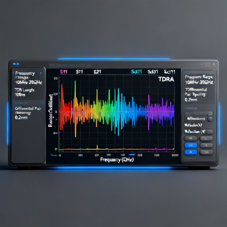
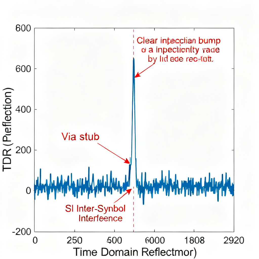
TDR sends a fast step pulse into the channel and measures reflections. It reveals impedance discontinuities (causes of reflections) that contribute to ISI. A TDR plot shows you exactly where the impedance changes (e.g., a via stub or connector mismatch). TDT measures the transmitted pulse at the receiver. A TDT plot shows the pulse’s rise time degradation, settling time, and any long tails—all direct indicators of ISI.
Bit Error Rate (BER) Testing
A BERT transmits a known pseudo-random bit sequence (PRBS) and counts errors. By sweeping the sampling point (voltage and time), you can create a BER contour (a 3D bathtub curve). The “bathtub” shape shows the margin: a narrow, steep bathtub indicates severe ISI.
Vector Network Analyzer (VNA) and S-Parameters
In the frequency domain, ISI correlates with the channel’s insertion loss (S21) and return loss (S11). Insertion loss: a steep roll-off above the Nyquist frequency (half the data rate) indicates a lossy channel that will cause ISI. For example, at 10 Gbps, the Nyquist frequency is 5 GHz. If S21 at 5 GHz is worse than -10 dB, expect significant ISI. Group delay variation: if different frequencies arrive at the receiver at different times (non-linear phase), this causes dispersion-induced ISI. A flat group delay is ideal.
Advanced Eye Diagram Analysis (EEA)
Tools like Keysight’s EDA software or Cadence’s Sigrity offer Eye Diagram Eye Contour analysis. These use statistical methods to predict the worst-case eye closure based on the channel’s impulse response. They can separate ISI from random jitter, giving you a clean picture of the deterministic ISI component.
Mitigation Strategies for ISI
Once you’ve detected ISI, the solution lies in both PCB design and signal processing.
PCB Material and Stackup Design
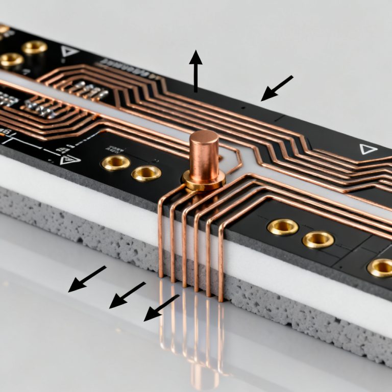
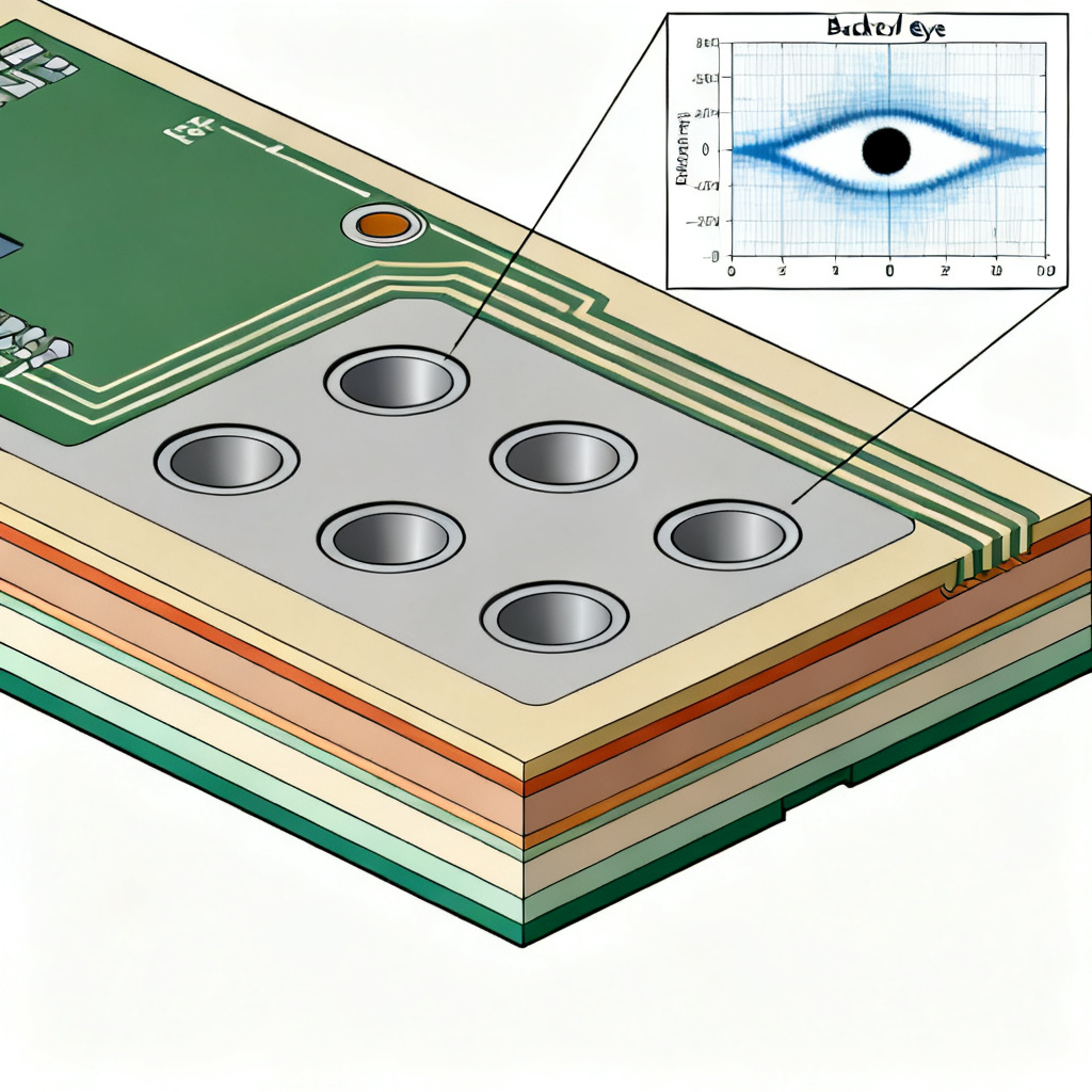
Choose low-loss materials: replace standard FR-4 with high-speed laminates like Rogers 4350B, Megtron 6, or Isola I-Tera. These have lower dielectric loss (Df) and more stable dielectric constant (Dk), reducing signal dispersion. Control impedance: use a tightly controlled stackup with microstrip or stripline geometries. Ensure impedance tolerance is within ±5% to minimize reflections. Reduce via stubs: use back-drilling to remove unused via stubs. A stub acts as a resonant cavity, causing frequency-dependent loss and reflections.
Equalization Techniques (At the IC Level)
Since you cannot always change the PCB, use equalization in the transceiver ICs. Pre-emphasis / De-emphasis (TX Equalization) boosts high-frequency components at the transmitter to compensate for channel loss. For example, a “pre-cursor” and “post-cursor” tap can cancel out the long tail of a pulse. Continuous Time Linear Equalizer (CTLE) (RX Equalization) is a high-pass filter at the receiver that amplifies attenuated high frequencies. Decision Feedback Equalizer (DFE) (RX Equalization) is a non-linear filter that subtracts the interference from previous bits. DFE is highly effective against ISI but can cause error propagation.
Routing and Layout Best Practices
Minimize trace length: keep high-speed traces as short as possible. Every inch of trace adds loss. Avoid right-angle bends: use 45-degree chamfered bends or curved traces to maintain impedance. Route over a continuous ground plane: avoid splits in the reference plane, which cause impedance changes. Use differential pairs: for high-speed serial links (e.g., PCIe, USB, Ethernet), use tightly coupled differential pairs. They are more immune to common-mode noise and have better return current paths.
Channel Simulation and Post-Layout Verification
Before fabrication, run post-layout simulations using tools like HyperLynx, SiSoft, or Cadence Sigrity. Simulate the eye diagram with a PRBS pattern. If the eye is closed, iterate on the design: reduce via stubs, improve impedance matching, or add equalization.
Case Study: Detecting ISI in a 25 Gbps Link
Scenario: A PCB for a 25 Gbps NRZ serial link shows a closed eye diagram during testing.
Observation: The eye diagram shows a “double eye” on the rising edge. The bathtub curve shows a BER floor at 1e-12.
Root Cause Analysis:
- TDR: Reveals a 10% impedance bump at a via transition (caused by a 15-mil via stub).
- S-Parameter: Insertion loss at 12.5 GHz (Nyquist) is -15 dB, exceeding the -10 dB limit.
- ISI Plot: Worst-case pattern is a “00000001” (a single ‘1’ after six ‘0’s), causing the slowest rising edge.
Solution:
- Back-drill the via stub to reduce its length by 80%.
- Change the PCB material from FR-4 to Megtron 6 (Df reduced from 0.025 to 0.002).
- Add a 3-tap DFE in the receiver IC.
Result: The eye diagram reopens to 60% height and 70% width. BER improves to <1e-15.
Frequently Asked Questions (FAQ)
What is ISI in high-speed PCB design?
Inter-Symbol Interference (ISI) in high-speed PCB design is a signal distortion phenomenon where the energy of one transmitted bit bleeds into subsequent bits, causing data-dependent errors and closing the eye diagram.
How does ISI affect eye diagrams?
ISI in eye diagrams appears as reduced eye height and eye width, a “fuzzy” or “thick” eye, and a “double eye” on rising edges. It introduces deterministic jitter that degrades signal integrity.
What are the main causes of ISI?
The main causes of ISI include channel bandwidth limitations, impedance discontinuities, skin effect, dielectric loss, and unintentional crosstalk between traces.
How can I detect ISI in my PCB?
You can detect ISI using time-domain reflectometry (TDR), bit error rate (BER) testing, vector network analyzer (VNA) measurements, and advanced eye diagram analysis (EEA) tools.
What are the best ways to mitigate ISI?
Mitigation strategies include using low-loss PCB materials, controlling impedance, reducing via stubs, implementing equalization techniques (pre-emphasis, CTLE, DFE), and following best routing and layout practices.
Comparison: Our High-Speed PCB Solutions vs. Standard Options
| Feature | Our High-Speed PCB (Optimized for ISI) | Standard PCB |
|---|---|---|
| PCB Material | Low-loss laminates (e.g., Megtron 6, Rogers) | Standard FR-4 |
| Impedance Control | ±5% tolerance, full stackup simulation | ±10% tolerance, basic control |
| Via Treatment | Back-drilling to remove stubs | No back-drilling |
| Equalization Support | Pre-emphasis, CTLE, DFE ready | Limited support |
| Simulation & Verification | Post-layout eye diagram, TDR, VNA analysis | Minimal simulation |
| Typical BER Improvement | <1e-15 | >1e-12 |
Glossary of Key Terms
- Inter-Symbol Interference (ISI): Signal distortion where one bit interferes with subsequent bits.
- Eye Diagram: An oscilloscope display showing overlapped bit periods to visualize signal quality.
- Deterministic Jitter (DJ): Jitter that is data-dependent and bounded, often caused by ISI.
- Time-Domain Reflectometry (TDR): A measurement technique using reflected pulses to find impedance discontinuities.
- Bit Error Rate (BER): The number of bit errors per unit time, used to quantify signal integrity.
- Insertion Loss (S21): The loss of signal power due to the channel.
- Decision Feedback Equalizer (DFE): A non-linear equalizer that subtracts interference from previous bits.