Master Reflection in Transmission Line Analysis for high-speed PCB designs using Cadence Sigrity. This practical guide covers TDR simulation, impedance discontinuities, termination strategies, and step-by-step workflows to ensure signal integrity for your advanced PCB projects.
Understanding the Physics of Reflection in High-Speed PCB
Before diving into software, you must grasp the fundamental principles. Reflection is governed by the reflection coefficient (Γ), defined as:
\[ \Gamma = \frac{Z_L – Z_0}{Z_L + Z_0} \]
Where:
- \( Z_0 \) = characteristic impedance of the transmission line (e.g., 50Ω)
- \( Z_L \) = load impedance or impedance at the discontinuity
Key implications for PCB designers:
- Open Circuit (Z_L = ∞): Γ = +1. Signal is fully reflected with the same polarity, causing overshoot.
- Short Circuit (Z_L = 0): Γ = -1. Signal is fully reflected with opposite polarity, causing undershoot.
- Matched Impedance (Z_L = Z_0): Γ = 0. No reflection. This is your target.
- Capacitive Discontinuity (e.g., via stub): Causes a negative reflection initially, followed by a positive one, creating ringing.
Why this matters for your high-speed PCB: Every impedance change—a via transitioning layers, a connector, a change in trace width, or a stub—creates a reflection. In a 50Ω system, a 60Ω via will reflect ~9% of the signal energy. At high frequencies, this small reflection can combine with others to cause eye closure.

Core Tools in Cadence Sigrity for Reflection Analysis
Cadence Sigrity provides a dedicated environment for SI analysis. The three primary tools for reflection analysis are:
2.1 Sigrity PowerSI
- Purpose: Extracts S-parameters and impedance profiles from PCB layouts.
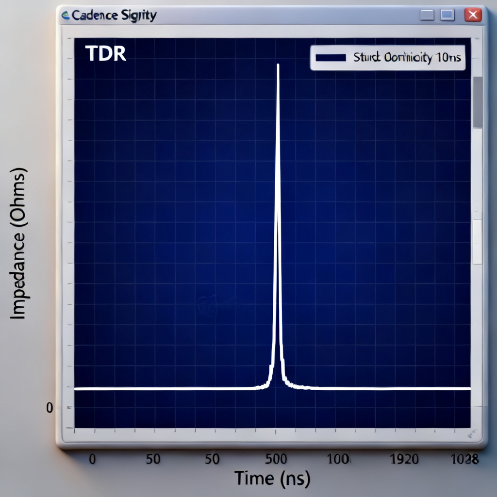
- Use Case: Run a TDR (Time Domain Reflectometry) simulation on a net to visualize where impedance discontinuities occur.
- Workflow:
- Import your layout (BRD/ODB++).
- Select the target net.
- Run a “TDR Impedance” simulation.
- Analyze the impedance vs. time plot. A flat line at 50Ω means good impedance control; spikes indicate discontinuities.
2.2 Sigrity SystemSI
- Purpose: Time-domain transient simulation for digital signals.
- Use Case: Simulate actual digital waveforms (e.g., PRBS pattern) on a net to see the effect of reflections on the eye diagram.
- Workflow:
- Set up a driver and receiver model (IBIS model).
- Define the net topology.
- Run a transient simulation.
- Examine the waveform for overshoot/undershoot and the eye diagram for eye height/width closure.
2.3 Sigrity OptimizePI
- Purpose: Automated optimization of termination and topology.
- Use Case: If you detect reflections, OptimizePI can sweep termination values (series, parallel, AC) to find the optimal solution.
- Workflow:
- Define design goals (e.g., max overshoot < 10%, eye height > 500mV).
- Set optimization variables (e.g., termination resistor value).
- Run the optimization. The tool will recommend the best termination strategy.
A Practical Step-by-Step Guide to Reflection Analysis in Cadence Sigrity
This section combines the most detailed workflows from the top sources.
Step 1: Set Up Your Simulation Environment
- Launch Sigrity PowerSI and import your PCB layout file.
- Select the high-speed net you want to analyze. For multi-drop buses, select the entire net topology.
- Define the frequency range. For reflection analysis, a range from DC to at least 5x the signal’s fundamental frequency is recommended (e.g., for a 1GHz clock, simulate up to 5GHz).
- Assign material properties. Ensure your dielectric constant (Dk) and loss tangent (Df) are accurate for your chosen laminate (e.g., FR-4, Rogers, Megtron).
Step 2: Run TDR Impedance Analysis
- Objective: Identify the physical location of impedance discontinuities.
- Action: In PowerSI, select the net and run a “TDR Impedance” simulation.
- Interpreting the TDR Plot:
- Flat line at 50Ω: Ideal.
- Upward spike: Inductive discontinuity (e.g., a narrow trace or a via with a long stub).
- Downward dip: Capacitive discontinuity (e.g., a wide pad or a via with a short stub).
- Gradual slope: Impedance taper or material variation.
- Pro Tip: Use the “Time-to-Distance” conversion in Sigrity to map the reflection to a physical location on the PCB. This allows you to zoom into the exact via or trace that is causing the problem.
Step 3: Simulate the Digital Waveform
- Objective: See how reflections affect the actual signal.
- Action: Switch to Sigrity SystemSI.
- Setup:
- Assign IBIS models to the driver and receivers.
- Set the data rate (e.g., 10Gbps) and pattern (e.g., PRBS7).
- Run a transient simulation.
- Interpreting the Waveform:
- Overshoot/Undershoot: A clear sign of reflection. Overshoot above the receiver’s absolute maximum rating can damage the IC.
- Ringing: Oscillations that persist after the signal edge. Caused by multiple reflections.
- Non-monotonic edges: The signal rises, then dips, then rises again. This can cause false clocking.
Step 4: Analyze the Eye Diagram
- Objective: Quantify signal quality.
- Action: In SystemSI, view the eye diagram.
- Key Metrics:
- Eye Height: The voltage margin. Must be above the receiver’s input threshold (e.g., > 200mV for LVDS).
- Eye Width: The timing margin. Must be greater than the setup/hold time.
- Jitter: Horizontal eye closure. Caused by reflections and crosstalk.
- Troubleshooting: If the eye is closed or has significant jitter, you have a reflection problem.
Step 5: Mitigate Reflections with Termination
- Objective: Match the impedance.
- Action: Use Sigrity OptimizePI or manual trial-and-error in SystemSI.
- Common Termination Strategies:
- Series Termination (Source Termination): Place a resistor (e.g., 22Ω) near the driver. This matches the driver’s output impedance to \( Z_0 \). Best for point-to-point traces.
- Parallel Termination (Load Termination): Place a resistor to GND or VTT at the receiver. This matches the load to \( Z_0 \). Best for single-ended lines.
- AC Termination: A capacitor in series with a parallel resistor. Blocks DC current while providing AC impedance matching.
- Thevenin Termination: Two resistors (e.g., 50Ω to VCC and 50Ω to GND). Best for differential pairs.
- Sigrity Optimization: Let OptimizePI sweep values for you. It will recommend the optimal resistor value and placement to minimize reflections.

Advanced Reflection Analysis Techniques in Cadence Sigrity
Beyond basic TDR and termination, top designers use these advanced techniques in Sigrity:
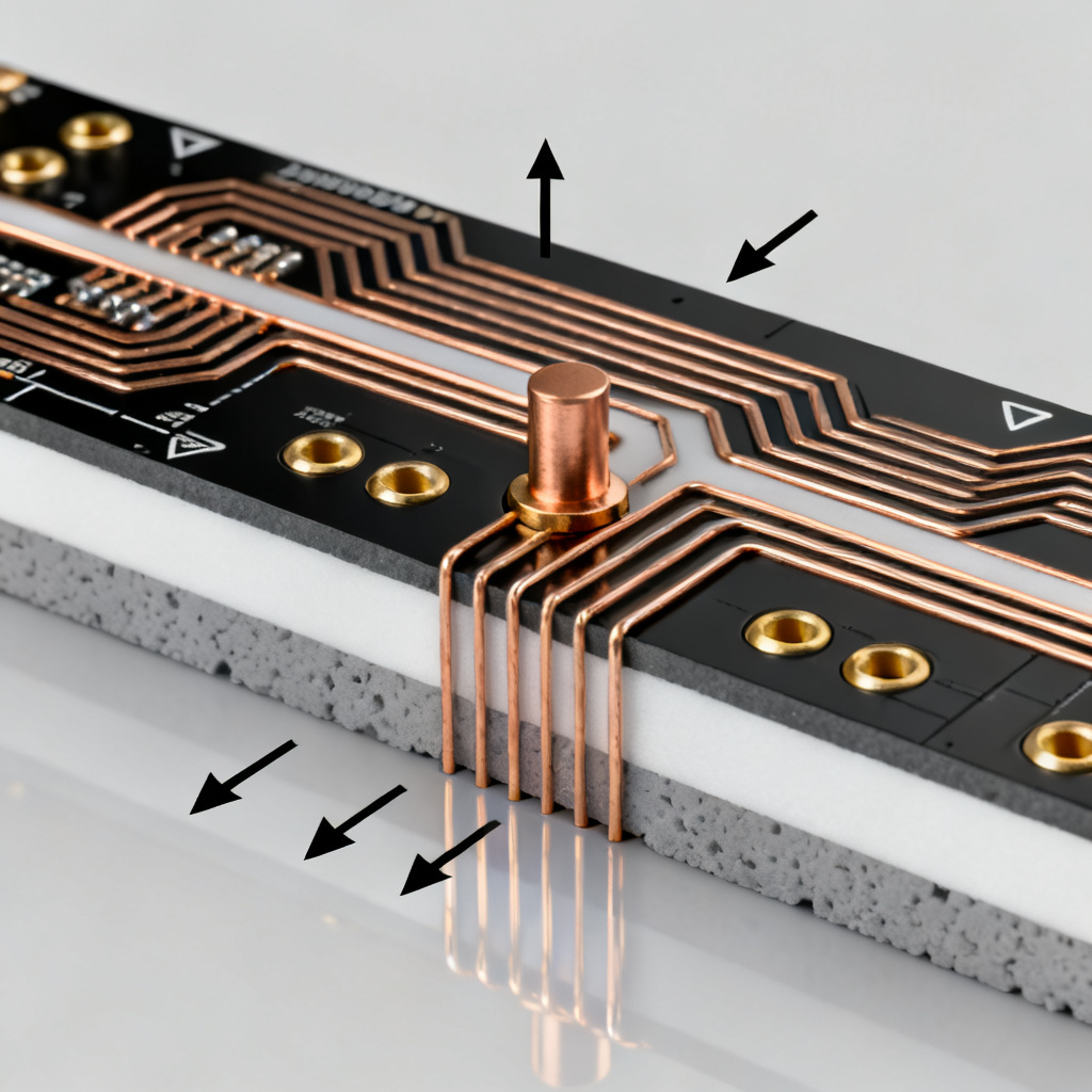
4.1 Analyzing Via Stubs
- Problem: A via stub (the unused portion of a via barrel) acts as a quarter-wave resonator. At certain frequencies, it creates a deep notch in the insertion loss and a severe reflection.
- Sigrity Solution: In PowerSI, extract the S-parameters for the via. Look for a dip in S21 (insertion loss). Use the “Via Stub Analysis” tool to calculate the resonant frequency. The fix: back-drill the via to remove the stub, or use a blind/buried via.
4.2 Multi-Reflection Analysis
- Problem: In a multi-drop bus (e.g., DDR memory), reflections from multiple receivers can constructively interfere.
- Sigrity Solution: In SystemSI, use the “Reflection Plot” feature. It shows the voltage waveform at multiple points along the line. You can see the incident wave, the reflected wave, and the sum. This helps you understand the timing of reflections.
4.3 Sensitivity Analysis
- Problem: Manufacturing tolerances (e.g., ±10% impedance) can cause reflections.
- Sigrity Solution: Use the “Design of Experiments (DOE)” feature in OptimizePI. Vary the trace width, dielectric thickness, and copper roughness. Run 100+ simulations to see the statistical distribution of reflections. This gives you a robust design that works even with real-world manufacturing variations.
Best Practices for High-Speed PCB Layout (Reflection Prevention)
Based on the combined wisdom from all sources, here are actionable layout guidelines for your high-speed PCB:
- Maintain Constant Impedance: Use a 50Ω (or 100Ω differential) stackup. Avoid changes in trace width. If you must change width, use a tapered transition.
- Minimize Via Stubs: For high-speed signals (e.g., 10Gbps+), always back-drill vias or use blind/buried vias.
- Keep Traces Short: The longer the trace, the more time reflections have to settle. Use the “critical length” rule: \( L_{crit} = \frac{t_r}{2 \times PD} \), where \( t_r \) is the rise time and PD is the propagation delay.
- Use Proper Return Paths: Ensure a solid ground plane directly under the signal trace. A gap in the ground plane creates a huge impedance discontinuity.
- Simulate Early, Simulate Often: Run TDR analysis in Sigrity during the pre-layout and post-layout phases. Fixing a reflection problem in the layout stage is far cheaper than fixing it on a prototype.
FAQ: Reflection in Transmission Line Analysis in Cadence Sigrity
What is the reflection coefficient in high-speed PCB design?
The reflection coefficient (Γ) quantifies how much signal energy is reflected at an impedance discontinuity. For a 50Ω system, a mismatch of 10Ω results in Γ ≈ 0.09, causing signal degradation.
How do I identify impedance discontinuities using Cadence Sigrity?
Use the TDR Impedance simulation in Sigrity PowerSI. A flat line at 50Ω indicates good impedance control, while spikes or dips reveal discontinuities like via stubs or trace width changes.
What is the best termination strategy for high-speed PCBs?
The optimal termination depends on the topology. Series termination is best for point-to-point traces, while parallel or Thevenin termination suits multi-drop buses. Use Sigrity OptimizePI to automatically find the ideal values.
How do via stubs affect signal integrity in high-speed designs?
Via stubs act as quarter-wave resonators, creating a deep notch in insertion loss and severe reflections. Back-drilling or using blind/buried vias in Cadence Sigrity can mitigate this issue.
Can Cadence Sigrity simulate multi-reflection effects?
Yes, the “Reflection Plot” feature in SystemSI shows waveforms at multiple points along the line, helping you understand how reflections constructively or destructively interfere.