Creating impedance control PCB test vehicles is a critical step in manufacturing validation for high-speed designs, ensuring signal integrity and production reliability. This guide covers coupon design, stack-up considerations, testing methodologies, and data analysis to help you validate your high-speed PCBs effectively.
1. Understanding Impedance Control and Why Test Vehicles Are Essential
1.1 What Is Impedance Control?
Impedance control refers to the consistent characteristic impedance of a transmission line along its entire length. For high-speed signals above 100 MHz or with fast rise times, mismatched impedance causes reflections, ringing, and data errors. Common target impedances are 50Ω for single-ended and 100Ω for differential pairs.
1.2 Why Test Vehicles Are Mandatory
Manufacturing processes such as etching, lamination, and prepreg flow introduce variations that can shift impedance by 5–15%.
- Process Variation Compensation: A test vehicle captures real-world effects to ensure consistent impedance.
- Verification of Stack-Up: The test vehicle confirms that the designed layer stack-up produces the intended impedance.
- Certification for High-Volume Production: Test vehicles provide statistical proof that the fabricator can hold impedance tolerances.
- Troubleshooting Signal Integrity Issues: If a final board fails, the test vehicle helps isolate whether the problem is design-related or manufacturing-related.
1.3 When to Use a Test Vehicle
- Prototype Phase: To validate a new stack-up or design rule.
- First Article Inspection: For the first production run of a new board.
- Process Qualification: When switching to a new PCB manufacturer or material set.
- Periodic Monitoring: For ongoing production quality assurance.
2. Designing the Impedance Control Test Vehicle
2.1 Coupon Design: The Heart of the Test Vehicle
A coupon is a small, dedicated test structure placed on the PCB panel used for impedance validation. Key design rules include:
- Length: Coupons should be at least 3 inches long to allow accurate TDR measurements.
- Width: The trace width must exactly match the designed impedance line width.
- Ground Planes: For stripline coupons, include solid ground planes above and below; for microstrip, include a solid ground plane below only.
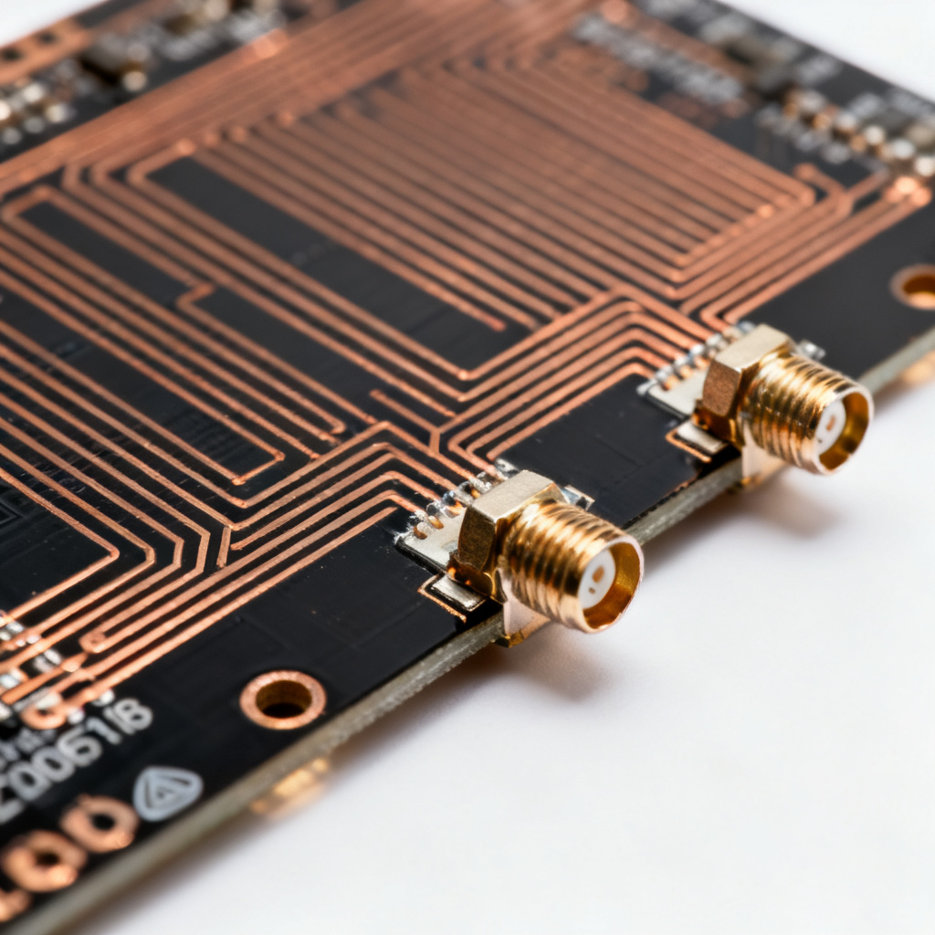
- Launch Points: Add test pads or SMA connectors at both ends for easy probe attachment.
- Multiple Coupons: Include separate coupons for single-ended microstrip, differential microstrip, single-ended stripline, and differential stripline.
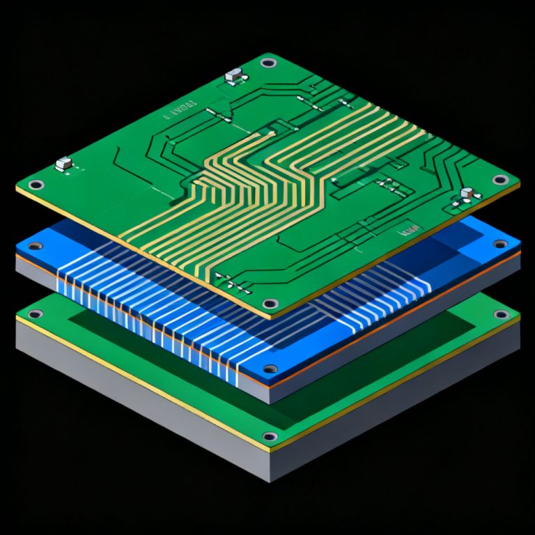
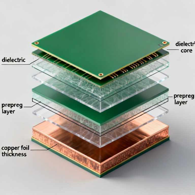
2.2 Stack-Up Considerations for Test Vehicles
The test vehicle must use the exact same stack-up as the production board, including core and prepreg materials, copper weight, layer count, and thickness tolerances. If the production board uses multiple impedance targets, the test vehicle must include coupons for each target.
2.3 Placement of Coupons on the Panel
- Edge Coupons: Place coupons along the panel edge to avoid warpage.
- Internal Coupons: For large panels, include coupons near the center to detect process variations across the panel.
- Separate Test Panel: For high-volume production, a dedicated test panel can be run alongside production panels.
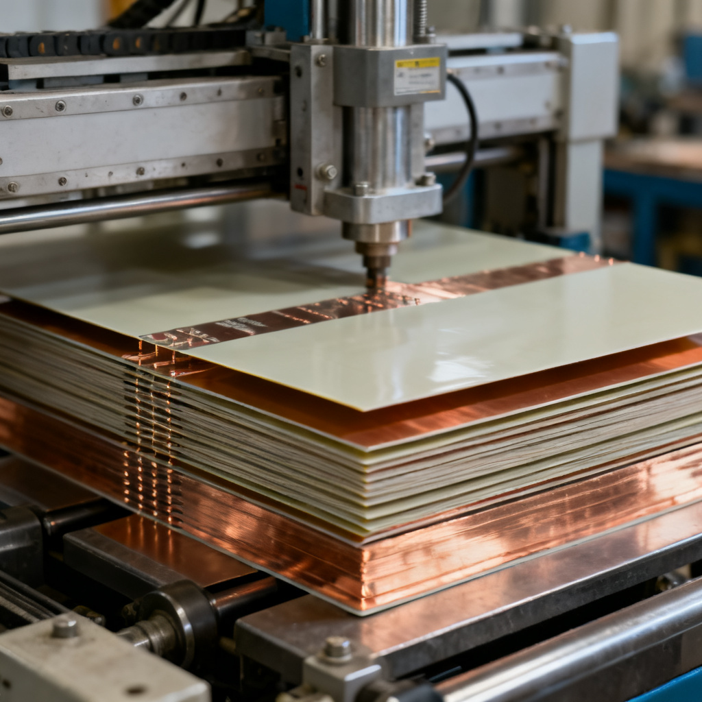
3. Manufacturing and Fabrication of Test Vehicles
3.1 Collaboration with the PCB Fabricator
Before sending the test vehicle design, provide clear specifications including target impedance values, trace widths, dielectric thicknesses, and material Dk/Df values. Request the fabricator to add the designed coupons to the production panel or run a separate test panel. Confirm acceptable impedance tolerances such as ±10% for standard or ±5% for tight control.
3.2 Fabrication Process Control Points
The test vehicle must go through the same fabrication steps as the production board, including lamination, etching, plating, and surface finish. Common mistakes to avoid include using different materials, ignoring resin flow, and misaligned layers.
3.3 Common Fabrication Mistakes to Avoid
- Using Different Materials: Even a slight change in prepreg type can shift impedance by 5–10%.
- Ignoring Resin Flow: Prepreg resin flow can reduce dielectric thickness by 10–20%.
- Misaligned Layers: For stripline, ensure the trace is centered between ground planes to avoid impedance shifts.
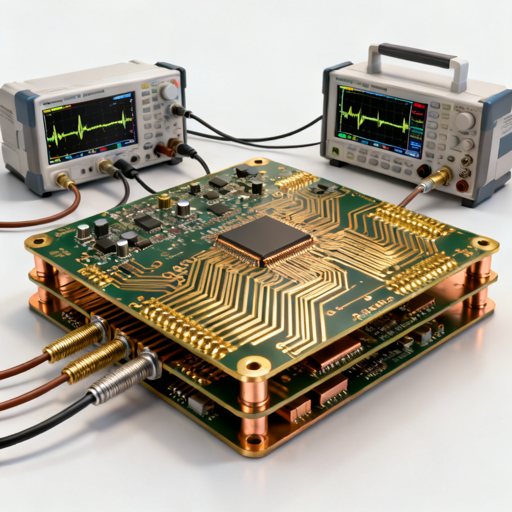
4. Testing the Impedance Control Test Vehicle
4.1 Test Methods: TDR vs. VNA
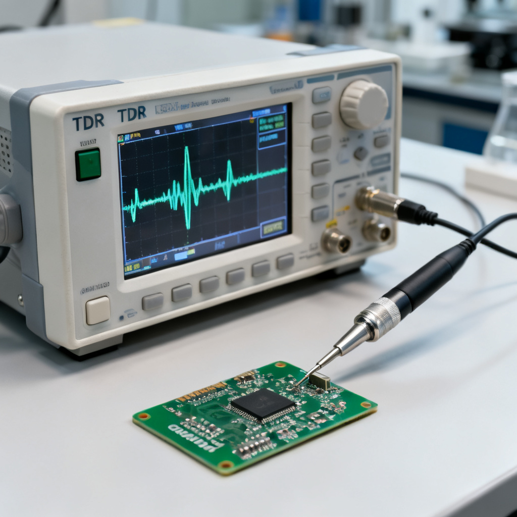
Time Domain Reflectometry (TDR) is the most common method, sending a fast rise-time pulse down the transmission line and measuring the reflected signal. Vector Network Analyzer (VNA) is better for higher frequencies and material characterization. TDR is recommended for manufacturing validation due to its speed and simplicity.
4.2 Measurement Setup and Best Practices
- Probe Selection: Use a 50Ω impedance-matched probe.
- Calibration: Perform a full calibration before each measurement session.
- Temperature Control: Measure at room temperature to avoid thermal effects.
- Multiple Measurements: Take at least 3 measurements per coupon and average them.
- Data Recording: Record measured impedance, trace width, and dielectric thickness for each coupon.
4.3 Interpreting Test Results
| Acceptance Criteria | Impedance Control Tolerance | Application |
|---|---|---|
| Standard Tolerance | ±10% of target impedance | General high-speed digital |
| Tight Tolerance | ±5% of target impedance | DDR5, PCIe Gen 5 |
| Premium Tolerance | ±3% of target impedance | RF/microwave applications |
When results fail, check the measurement setup, analyze the coupon design, review fabrication data, and identify the root cause. Common causes include over-etching, under-etching, incorrect dielectric thickness, or wrong material Dk.
5. Advanced Topics and Best Practices
5.1 Including Test Structures for Material Characterization
Beyond impedance, a test vehicle can include ring resonators for measuring Dk and Df, transmission lines of varying lengths for extracting attenuation, and crosstalk coupons to validate adjacent trace isolation.
5.2 Statistical Process Control for Production
Use test vehicle data to create control charts, monitor trends, and take corrective action when impedance drifts beyond control limits.
5.3 Design of Experiments for Process Optimization
Run a DOE to identify which variables such as trace width, trace spacing, dielectric thickness, and lamination pressure have the most significant impact on impedance.
5.4 Common Pitfalls and How to Avoid Them
| Pitfall | Consequence | Solution |
|---|---|---|
| Using a single coupon for multiple impedance targets | Inaccurate readings due to coupling | Design separate coupons for each target |
| Ignoring launch effects | Impedance spikes at coupon ends | Measure only the middle 50% of the coupon |
| Not accounting for soldermask | Soldermask lowers impedance by 1–3 Ω | Include soldermask on the coupon if used on production board |
| Using a different test method than the fabricator | Discrepancies in reported impedance | Agree on a single test method and calibration standard |
| Failing to document the test vehicle design | Unable to reproduce results | Create a detailed test vehicle specification document |
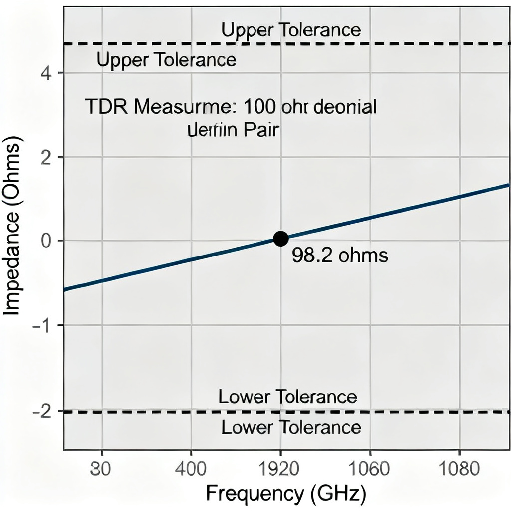
6. Case Study: Validating a 100Ω Differential Pair for PCIe Gen 5
A customer needed a 16-layer PCB with a 100Ω differential pair for PCIe Gen 5. The test vehicle included a 100Ω differential stripline coupon with trace width 4.5 mil, gap 6 mil, and dielectric thickness 3.5 mil above and below. TDR measurement showed 98.2 Ω differential impedance, single-ended traces at 49.8 Ω and 50.1 Ω, and crosstalk at -42 dB at 16 GHz. All values were within ±5% tolerance, confirming the fabricator’s capability.
7. Conclusion: Making Test Vehicles a Standard Practice
Creating impedance control PCB test vehicles is a critical quality assurance process that ensures high-speed designs work in the real world. By designing proper coupons, collaborating with the fabricator, measuring accurately with TDR or VNA, and analyzing data, you can catch manufacturing variations early, avoid costly redesigns, and deliver reliable high-speed PCBs. Always include test vehicles for new designs and material changes, standardize coupon design, and document everything for future reference.