In high-speed PCB design, jitter is the critical timing deviation that determines signal integrity and system reliability. This pillar content explores jitter in high speed PCB simulation in Ansys HFSS, detailing what the tool can and cannot achieve for accurate jitter analysis.
Understanding Jitter in High Speed PCB Design
What Is Jitter and Why Does It Matter for Your High Speed PCB?
Jitter in high speed PCB design refers to the time-domain variation of a signal edge from its ideal position. It directly impacts bit error rate (BER) and is a primary concern for protocols like PCIe 5.0, DDR5, and 100G Ethernet. Jitter is categorized into random jitter (RJ) and deterministic jitter (DJ), with DJ further split into periodic jitter (PJ), data-dependent jitter (DDJ), and duty-cycle distortion (DCD). For B2B PCB manufacturers, controlling jitter in high speed PCB simulation is essential to deliver reliable boards.
Key jitter sources in a high speed PCB include channel loss from skin effect and dielectric absorption, impedance discontinuities at vias and connectors, crosstalk from adjacent traces, power integrity noise, and manufacturing tolerances in dielectric constant (Dk) and trace width. Each of these contributes to the overall jitter budget that must be managed through simulation and design optimization.
What Ansys HFSS Can Do for Jitter in High Speed PCB Simulation
Extracting S-Parameters for Passive Channel Analysis
Ansys HFSS excels at modeling passive interconnects with 3D full-wave EM simulation. It computes S-parameters for traces, vias, connectors, and packages, capturing insertion loss, return loss, and crosstalk. These frequency-domain data are fundamental for jitter in high speed PCB simulation, as they allow time-domain conversion to observe DDJ and ISI.
Generating TDR Profiles and Eye Diagrams
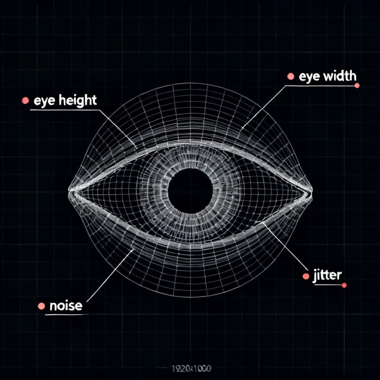
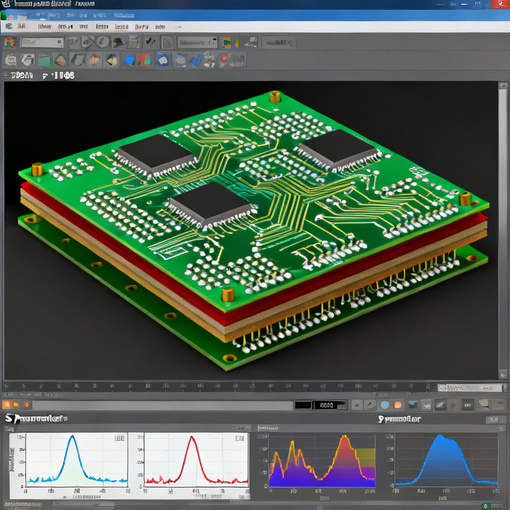
HFSS can simulate TDR impedance profiles to identify discontinuities that cause reflections and jitter. Through integration with Ansys Designer, eye diagrams are generated from S-parameters, quantifying deterministic jitter (DDJ and crosstalk). This is a core capability for jitter in high speed PCB simulation, enabling engineers to visualize signal degradation.
Channel Operating Margin (COM) and Statistical Analysis
For standards like IEEE 802.3bj, COM analysis relies on HFSS S-parameters. The tool also supports parametric sweeps to model manufacturing tolerances, providing a range of DJ values. These features make HFSS indispensable for jitter in high speed PCB simulation, but they are limited to passive components.
What Ansys HFSS Cannot Do for Jitter in High Speed PCB Simulation
Active Jitter Sources Are Outside HFSS Scope
HFSS is a passive EM solver and cannot simulate random jitter from active circuits (e.g., thermal noise in drivers) or periodic jitter from power supply ripple. For jitter in high speed PCB simulation, these active components require circuit-level tools like SPICE or IBIS-AMI models in Ansys Designer.
No Direct Total Jitter Output
Total jitter (TJ) = DJ + RJ, where RJ is unbounded. HFSS only provides deterministic jitter from passive channels. To compute TJ for jitter in high speed PCB simulation, engineers must combine HFSS results with active jitter data from external sources or post-processing scripts.
Limited to Passive Interconnect Jitter
HFSS does not simulate DCD from driver asymmetry, jitter from termination mismatches, or non-ideal return paths unless explicitly modeled. It also cannot handle long bit sequences efficiently, making statistical eye methods preferable for jitter in high speed PCB simulation.
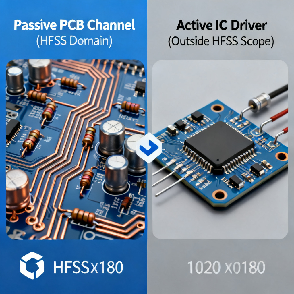
| Jitter in High Speed PCB Simulation Aspect | What HFSS Can Do | What HFSS Cannot Do |
|---|---|---|
| Passive channel S-parameters | Extract insertion loss, return loss, crosstalk | Simulate active driver noise |
| Time-domain eye diagram | Generate eye from S-parameters (DJ only) | Output total jitter (TJ) directly |
| Manufacturing tolerance impact | Parametric sweeps for DJ range | Model DCD from driver asymmetry |
| Standards compliance (COM) | Provide passive channel data | Simulate long PRBS patterns efficiently |
Best Practices for Jitter in High Speed PCB Simulation Using HFSS
Combine HFSS with Circuit-Level Simulation
For accurate jitter in high speed PCB simulation, use HFSS for passive S-parameters and import them into Ansys Designer with IBIS-AMI models. This captures both passive (DDJ, crosstalk) and active (RJ, PJ) jitter components.
Use Statistical Eye Analysis for Long Patterns
Statistical eye methods leverage HFSS S-parameters to compute jitter efficiently without transient simulation of long bit sequences. This is a practical approach for jitter in high speed PCB simulation at 28 Gbps and above.
Include Crosstalk and Manufacturing Tolerances
Simulate multiple aggressor lines in HFSS to capture crosstalk-induced jitter. Use parametric sweeps for Dk, trace width, and dielectric thickness to estimate worst-case jitter in high speed PCB simulation.
Leverage Power Integrity Co-Simulation
For periodic jitter from power supply noise, use Ansys SIwave to model PDN impedance and SSN. Couple this with HFSS channel models in Designer for a complete jitter in high speed PCB simulation workflow.
Practical Case Study: Jitter in High Speed PCB Simulation for 28 Gbps Channel
Step-by-Step Jitter Analysis Using HFSS
Consider a 28 Gbps backplane channel with a 12-inch trace, two vias, and a connector. For jitter in high speed PCB simulation, first create a 3D HFSS model with FR4 material (Dk=4.2, loss tangent=0.02) and copper roughness (0.5 μm RMS). Sweep S-parameters from DC to 40 GHz. Results show insertion loss of -8 dB at Nyquist frequency and crosstalk of -25 dB from an adjacent aggressor.
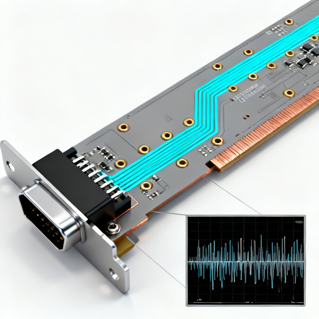
In Ansys Designer, apply a PRBS7 pattern to the channel. The eye diagram reveals deterministic jitter of 0.15 UI (from DDJ and crosstalk). Add an IBIS-AMI transmitter model with RJ=0.05 UI (rms) and PJ=0.03 UI. Total jitter (TJ) = DJ + 14*RJ = 0.85 UI, exceeding the typical 0.6 UI budget. Optimization through back-drilling and increased trace width reduces DJ to 0.10 UI, but equalization (CTLE) is still required. This case demonstrates that jitter in high speed PCB simulation with HFSS accurately predicts passive DJ, but active jitter must be added externally.
Frequently Asked Questions About Jitter in High Speed PCB Simulation in Ansys HFSS
Can HFSS simulate random jitter for my high speed PCB?
No, HFSS cannot simulate random jitter. Random jitter originates from active components like drivers and oscillators, requiring circuit-level tools. For complete jitter in high speed PCB simulation, combine HFSS passive results with IBIS-AMI models.
How do I get total jitter from HFSS for high speed PCB design?
HFSS provides deterministic jitter (DDJ, crosstalk) from passive channels. To obtain total jitter, you must add random jitter from active sources using post-processing or tools like Ansys Designer. This is a critical step for accurate jitter in high speed PCB simulation.
What are the main limitations of HFSS for jitter analysis in high speed PCBs?
The main limitations are that HFSS cannot simulate active jitter, cannot output total jitter directly, and is inefficient for long bit sequences. It is best used as a passive channel engine for jitter in high speed PCB simulation.
Can HFSS model crosstalk-induced jitter for high speed PCBs?
Yes, HFSS can model crosstalk by simulating multiple aggressor lines and extracting coupling S-parameters. This data is then used in time-domain analysis to quantify crosstalk jitter, a key part of jitter in high speed PCB simulation.
What is the best workflow for jitter in high speed PCB simulation using Ansys tools?
The best workflow is: (1) Extract S-parameters in HFSS for passive interconnects; (2) Import into Ansys Designer with IBIS-AMI models; (3) Perform statistical eye or transient simulation; (4) Add power integrity data from SIwave for complete jitter analysis. This approach maximizes accuracy for jitter in high speed PCB simulation.