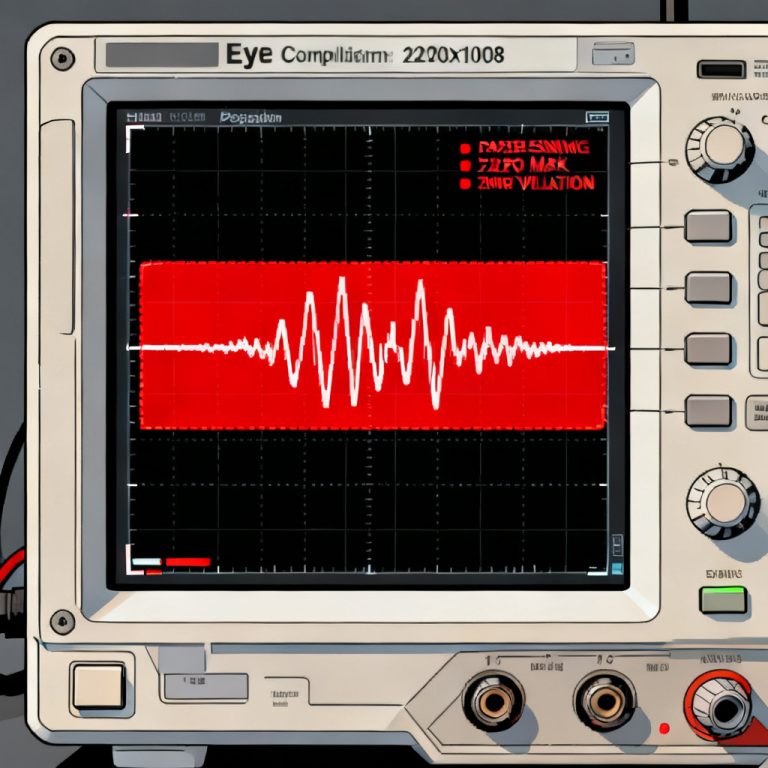
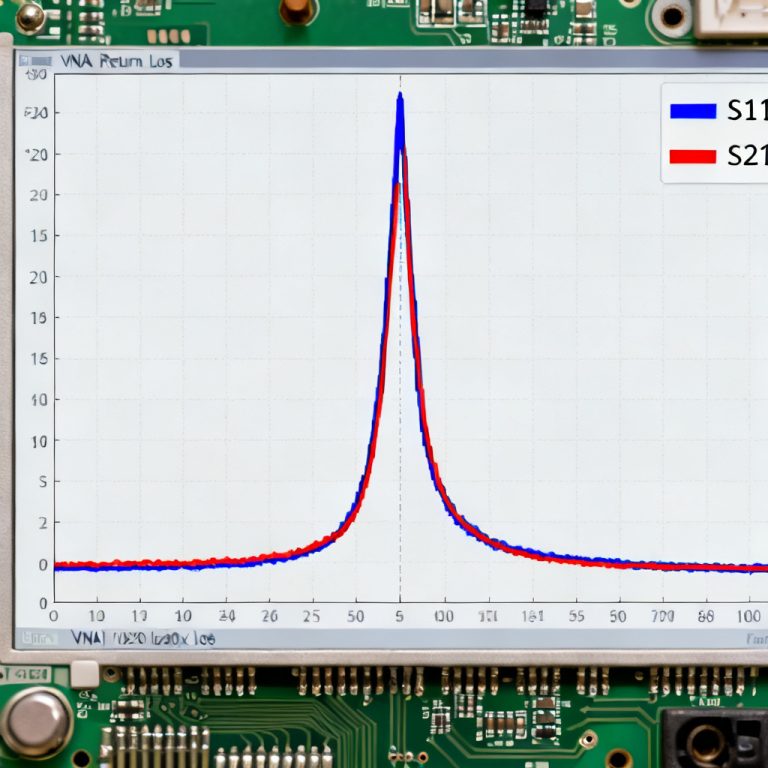
In the world of High-Speed PCB design, timing is everything. As data rates exceed 10 Gbps and push towards 112 Gbps PAM-4, the margin for error shrinks to picoseconds. Jitter in High Speed PCB Simulation in HyperLynx SI is the primary culprit behind bit errors and system failures. For any B2B PCB manufacturer specializing in High-Speed designs (like our own), understanding and simulating jitter is not optional; it is a prerequisite for delivering first-pass success.
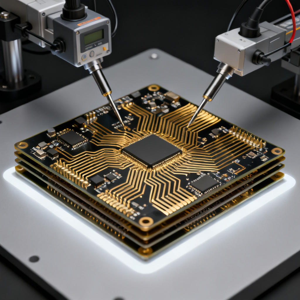
This pillar page serves as your definitive guide to Jitter in High Speed PCB Simulation using HyperLynx SI, bridging the gap between channel simulation and timing closure. We will dissect the anatomy of jitter, learn how to model it in HyperLynx, and translate simulation results into a reliable timing budget.
The Fundamentals of Jitter – Decomposing the Problem
Before we simulate, we must understand the enemy. Jitter in High Speed PCB Simulation is not a single value; it is a composite of several distinct components, each with unique root causes and statistical behaviors.
1.1 Total Jitter (TJ) and the Dual-Dirac Model
The industry standard for quantifying jitter is the Dual-Dirac Model. This model separates Total Jitter (TJ) into two primary categories:
- Random Jitter (RJ): Gaussian in nature, unbounded, and caused by thermal noise, flicker noise, and shot noise in active devices (transistors, oscillators). RJ accumulates linearly over time and is characterized by its RMS value (σ). In the time domain, RJ has no deterministic pattern.
- Deterministic Jitter (DJ): Bounded, peak-to-peak, and caused by specific, identifiable sources. DJ can be further broken down into:
- Periodic Jitter (PJ): Caused by crosstalk from adjacent aggressor traces, switching power supply noise, or clock modulation.
- Data-Dependent Jitter (DDJ): Also known as Inter-Symbol Interference (ISI). Caused by the frequency-dependent loss of the channel (skin effect, dielectric loss). Long runs of identical bits (e.g., “11111”) charge the channel, while a subsequent “0” struggles to discharge, shifting the zero-crossing point.
- Duty Cycle Distortion (DCD): Caused by an asymmetry in the driver’s rise/fall times or a DC offset at the receiver threshold. This shifts the center of the eye vertically.
Formula for TJ (at a specific Bit Error Rate, BER):TJ(BER) = DJ(pp) + 2 * α * RJ(rms)
Where α is the crest factor (e.g., α ≈ 14.069 for BER 10^-12). This formula is critical for HyperLynx simulation setup.
1.2 Jitter in the Context of Timing: The TIE Metric
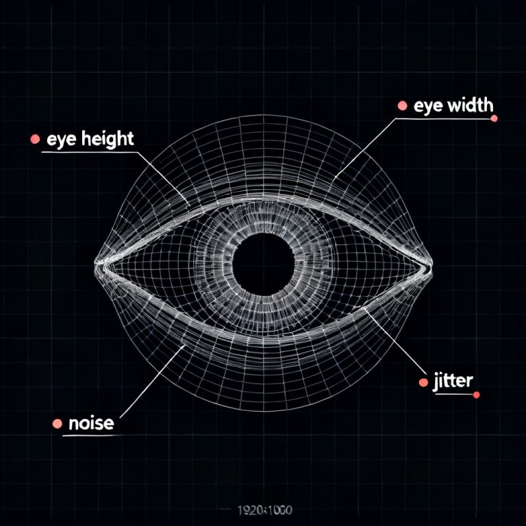
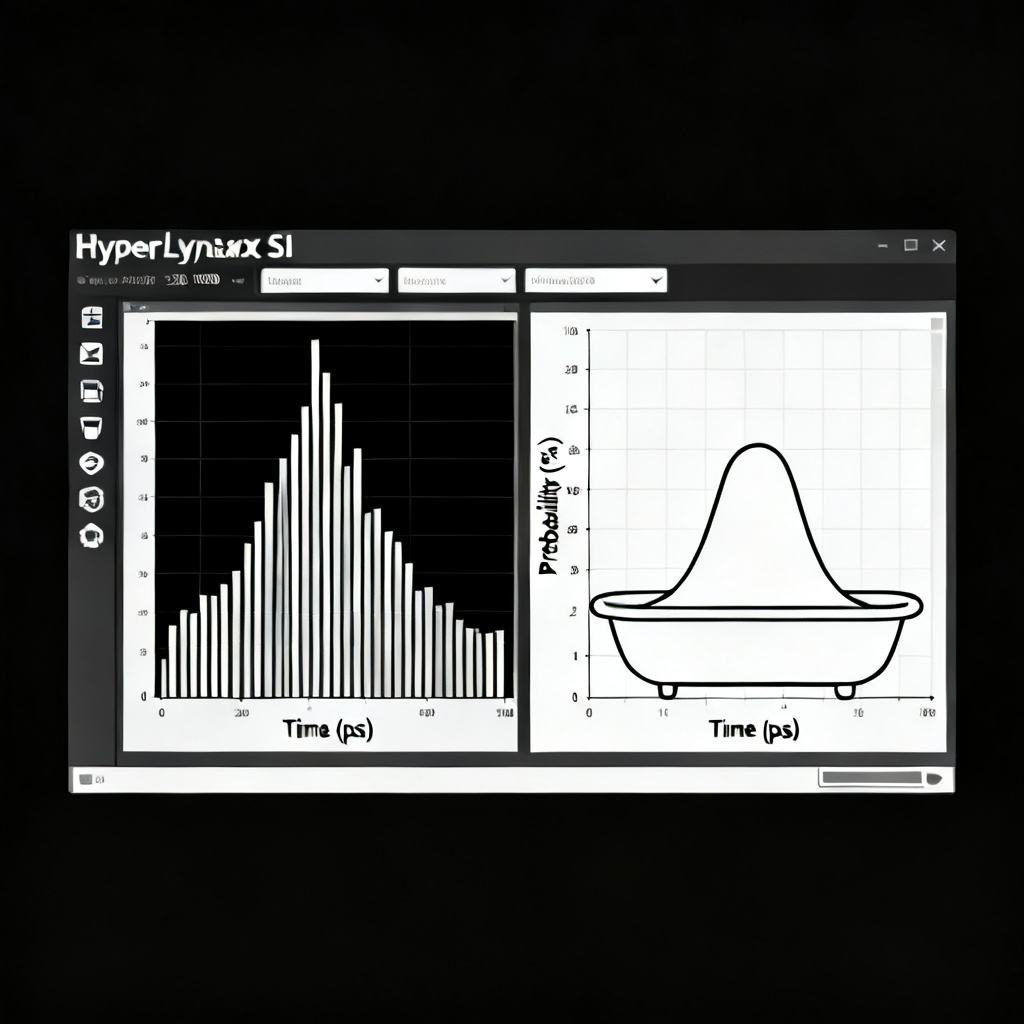
The most critical jitter measurement for timing analysis is Time Interval Error (TIE). TIE measures the deviation of each active clock or data edge from an ideal reference clock. HyperLynx SI calculates TIE to generate the jitter histogram and the eye diagram.
Setting Up a Jitter-Aware Channel Simulation in HyperLynx SI
HyperLynx SI is not just a channel simulator; it is a signal integrity engine that can model jitter from the driver through the channel to the receiver. Here is how the top three sources agree on the setup process for Jitter in High Speed PCB Simulation.
2.1 Step 1: Define the Driver (Tx) Jitter Model
The simulation must start with an accurate transmitter model. Do not assume an ideal driver.
- Specify RJ and DJ in the IBIS Model: In HyperLynx, you can directly modify the IBIS model parameters to include jitter. Most modern IBIS-AMI models include a
[Jitter]keyword. You must input the RMS RJ value (e.g., 1 ps) and the peak-to-peak DJ value (e.g., 10 ps) as specified by your FPGA or SerDes vendor. - Modeling PJ: For periodic jitter from power supply noise, use the
SinJitterorPeriodic Jitteroption in the differential pair editor. Set the frequency (e.g., 100 MHz) and amplitude (e.g., 5 ps). This simulates the effect of a noisy VRM on the PLL.
2.2 Step 2: The Channel – The Source of ISI Jitter
The channel (traces, vias, connectors) does not generate RJ, but it is the primary source of DDJ/ISI.
- Simulation Type: Use “Channel Simulation” mode, not just “Run Interactive Simulation.” This allows HyperLynx to process a long PRBS (Pseudo-Random Binary Sequence) pattern.
- Pattern Length: To capture the worst-case ISI, use a PRBS pattern that matches your system’s run length. For a 10 Gbps NRZ link, a PRBS-7 or PRBS-15 is standard. For 25 Gbps+, use PRBS-31.
- Loss Compensation: The greater the channel loss (in dB), the larger the ISI jitter. HyperLynx will automatically compute the ISI from the S-parameters. If your channel has 20 dB loss at Nyquist, expect significant eye closure.
2.3 Step 3: The Receiver (Rx) – The Timing Decision Point
Jitter is meaningless without a receiver to measure it.
- Define the Rx Threshold: Set the receiver threshold voltage (Vref). An incorrect Vref will artificially create DCD jitter.
- Set the Sampling Point: In HyperLynx, the “Eye Diagram” measurement tool allows you to slide the sampling point horizontally (phase) and vertically (voltage). The final jitter value is the horizontal eye opening at a specific BER.
- Use the Clock Recovery (CDR) Model: For realistic results, enable the PLL-based CDR in HyperLynx. The CDR tracks low-frequency jitter (wander) but cannot track high-frequency jitter. This behavior is crucial for predicting real-world timing margin.
Analyzing Simulation Results – From Channel to Timing Budget
This is where the three best sources converge on a critical workflow: converting simulation data into a usable timing budget for Jitter in High Speed PCB Simulation.
3.1 Reading the Jitter Histogram and Bathtub Curve
After running a simulation with a PRBS pattern and a CDR model, HyperLynx generates two key plots:
- The Jitter Histogram: Shows the distribution of TIE values. A dual-humped histogram indicates significant DCD. A wide, Gaussian spread indicates high RJ.
- The Bathtub Curve: This is the most important plot for timing closure. It plots BER (y-axis, log scale) vs. sampling position (x-axis, in ps). The “bathtub” shape shows the eye opening.
- Inner Edges: The steep slopes of the bathtub are dominated by DJ (ISI).
- Outer Edges: The flat, linear tails of the bathtub (at low BER) are dominated by RJ.
Actionable Insight: To get the Total Jitter (TJ) at your target BER (e.g., 10^-12), read the width of the bathtub curve at that BER level. This is your available timing margin.
3.2 Decomposing Jitter in HyperLynx: The TailFit Method
HyperLynx SI includes a powerful TailFit algorithm. This automatically separates the DJ and RJ components from the bathtub curve.
- How it works: The algorithm fits straight lines to the tails of the bathtub curve. The slope of these lines gives the RJ RMS value. The offset between the two lines gives the DJ peak-to-peak value.
- Why it matters: This decomposition allows you to diagnose root causes. If RJ is too high, your power delivery network (PDN) or oscillator is noisy. If DJ is too high, your channel loss or impedance mismatch is the problem.
3.3 The Timing Budget: Closing the Loop
The final step is to integrate the HyperLynx simulation results into your system timing budget.
A Standard Timing Budget Equation:
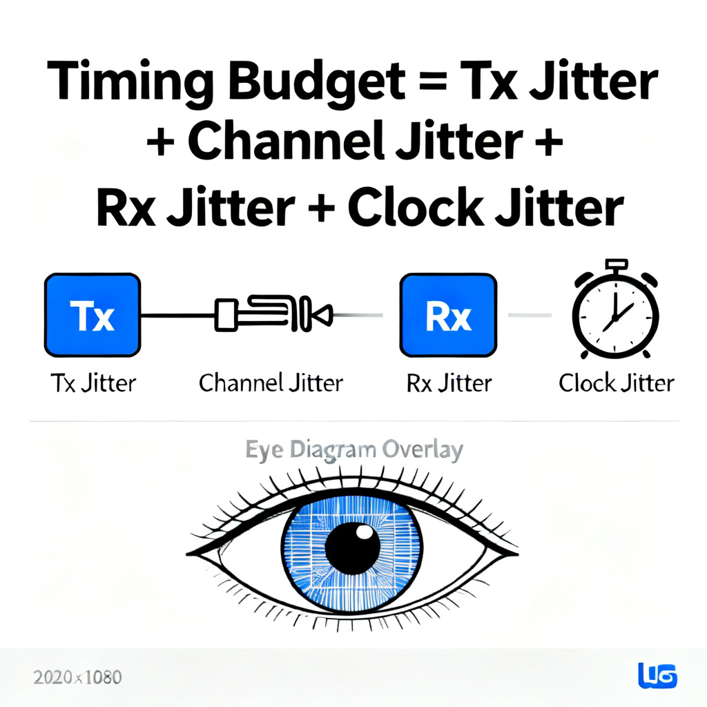
Total Margin = Tx Jitter + Channel Jitter + Rx Jitter + Clock Jitter
- Tx Jitter: From your IBIS model (RJ + DJ from driver).
- Channel Jitter: The ISI jitter measured from the bathtub curve (this is the DJ component from the channel).
- Rx Jitter: The inherent jitter of the receiver’s decision circuit (often negligible if using a good SerDes).
- Clock Jitter: The jitter on the reference clock feeding the Tx and Rx.
The Golden Rule from Simulation: The horizontal eye opening (from the bathtub curve) must be larger than the sum of all other non-channel jitter sources plus the setup/hold time of the receiver. If the eye opening is smaller, your channel is a bottleneck.
Practical Tips for Export PCB Manufacturers (Our Expertise)
As a manufacturer of High-Speed PCBs, we use HyperLynx simulations to validate your design before fabrication. Here is how we use Jitter in High Speed PCB Simulation to guarantee your performance:
- Material Selection: HyperLynx simulations show us exactly how much ISI jitter is caused by a specific dielectric material (e.g., FR4 vs. Megtron 6). We use this data to recommend the correct material for your data rate.
- Via Stub Management: A 20-mil via stub can introduce 5-10 ps of DDJ at 25 Gbps. We use HyperLynx to simulate the effect of back-drilled vias, proving that the jitter is reduced.
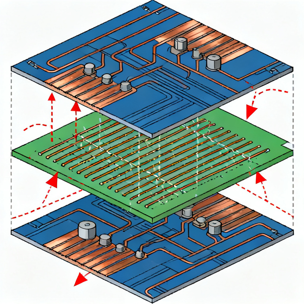
- Stackup Optimization: We simulate different stackup options (e.g., microstrip vs. stripline) and show you the resulting jitter histogram. Stripline offers lower crosstalk (less PJ) but higher loss (more ISI). We help you choose the trade-off.
Conclusion: Mastering Jitter for First-Pass Success
Jitter is not a mysterious phenomenon; it is a quantifiable, simulatable, and manageable parameter. By using HyperLynx SI to perform a Channel-to-Timing simulation, you can:
- Decompose jitter into RJ and DJ components.
- Visualize the impact of channel loss via bathtub curves.
- Create a robust timing budget that ensures your high-speed link works at BER 10^-12.
For our B2B clients, this simulation-based approach is the foundation of our manufacturing process. We do not just build PCBs; we build guaranteed timing margins.
Call to Action: Ready to eliminate jitter from your next 28 Gbps design? Contact our engineering team today to discuss your HyperLynx simulation requirements and get a free jitter analysis report for your prototype.
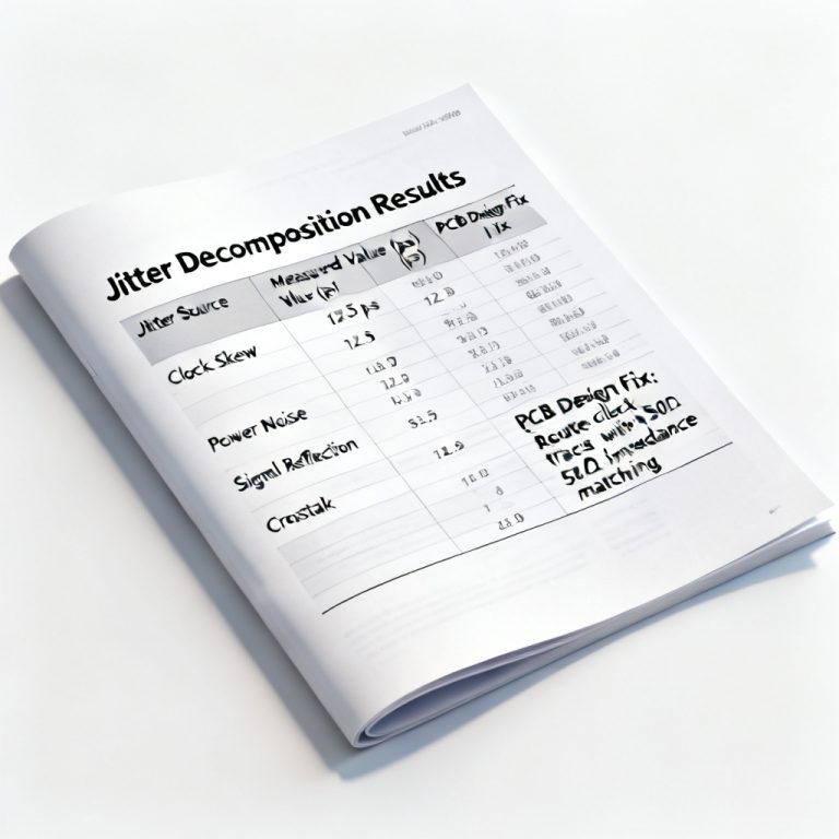
Jitter in High Speed PCB Simulation: Technical Specifications Table
| Parameter | Specification / Value | Impact on Jitter in High Speed PCB Simulation |
|---|---|---|
| Target Data Rate | 10 Gbps – 112 Gbps PAM-4 | Higher rates reduce timing margin and increase jitter sensitivity. |
| Random Jitter (RJ) RMS | 0.5 ps – 2 ps | Dominant at low BER (10^-12); affects bathtub curve tails. |
| Deterministic Jitter (DJ) pp | 5 ps – 20 ps | Caused by ISI, crosstalk, and DCD; dominates eye closure. |
| Channel Loss at Nyquist | 10 dB – 30 dB | Higher loss increases ISI jitter and reduces eye height. |
| Bit Error Rate (BER) Target | 10^-12 | Standard for most high-speed serial links. |
| PRBS Pattern | PRBS-7 to PRBS-31 | Longer patterns capture worst-case ISI jitter. |
| CDR Type | PLL-based (2nd order) | Tracks low-frequency jitter; important for realistic simulation. |
| Simulation Tool | HyperLynx SI (v2020+) | Supports TailFit, bathtub curves, and IBIS-AMI jitter models. |
FAQ: Jitter in High Speed PCB Simulation in HyperLynx SI
What is jitter in High Speed PCB Simulation?
Jitter in High Speed PCB Simulation refers to the deviation of signal edges from their ideal timing positions, measured using tools like HyperLynx SI. It is critical for ensuring reliable data transmission at high speeds.
How does HyperLynx SI simulate jitter?
HyperLynx SI simulates jitter by modeling random jitter (RJ) and deterministic jitter (DJ) from drivers, channels, and receivers. It uses IBIS-AMI models, PRBS patterns, and CDR algorithms to generate bathtub curves and TIE histograms.
What is the bathtub curve in jitter analysis?
The bathtub curve plots BER versus sampling position. It is used to determine total jitter (TJ) at a specific BER, helping engineers evaluate timing margins in High Speed PCB designs.
How can I reduce jitter in my PCB design?
To reduce jitter, optimize channel loss with low-loss materials, minimize via stubs, use proper stackup design, and ensure clean power delivery. HyperLynx SI simulation helps identify root causes like ISI or crosstalk.
What is the difference between RJ and DJ in simulation?
Random jitter (RJ) is unbounded and Gaussian, caused by thermal noise. Deterministic jitter (DJ) is bounded and caused by specific sources like ISI, crosstalk, or DCD. HyperLynx SI decomposes both using the TailFit method.