Master impedance control PCB for BGA breakout routing. Explore critical design strategies, material selection, and manufacturing techniques to ensure signal integrity in high-density PCB layouts. This guide delivers expert insights for consistent performance.
Section 1: The Fundamentals of Impedance Control in BGA Breakout
Controlled impedance is the management of the characteristic impedance of a transmission line, which is determined by the geometry of the trace and the properties of the surrounding dielectric materials. For a microstrip or stripline, the key variables are trace width, trace thickness, distance to the reference plane, and the dielectric constant (Dk) of the substrate.
In a BGA breakout area, these variables become extremely difficult to control simultaneously. The primary challenge is the density constraint. The BGA pitch (e.g., 0.8mm, 1.0mm, 0.5mm) forces trace widths and spacings to shrink dramatically. A typical 50-ohm microstrip on standard FR-4 might require a 10-12 mil trace width. But inside a fine-pitch BGA, the available channel width (the space between two adjacent BGA pads) might only be 4-6 mils.
This forces designers to use much narrower traces (e.g., 3-4 mils) in the breakout region. These narrow traces have a higher characteristic impedance than the wider traces used outside the BGA. The sudden transition from a narrow trace inside the BGA to a wider trace in the outer layers creates an impedance discontinuity, which acts like a small capacitor or inductor, reflecting energy back toward the source.
Key Insight from Industry Experts: The impedance in the breakout area is not a single value; it is a gradient. The trace impedance changes as it transitions from the BGA pad (where it is influenced by the pad’s capacitance) through the narrow channel, and then into the wider routing channel. The goal is to minimize the magnitude of this gradient.
Section 2: Critical Design Strategies for BGA Breakout Impedance Consistency
To maintain consistent impedance in dense BGA areas, designers must employ a combination of layer stackup planning, trace geometry optimization, and via management. The following strategies are derived from the most effective real-world designs.
2.1 Optimized Layer Stackup and Reference Plane Management
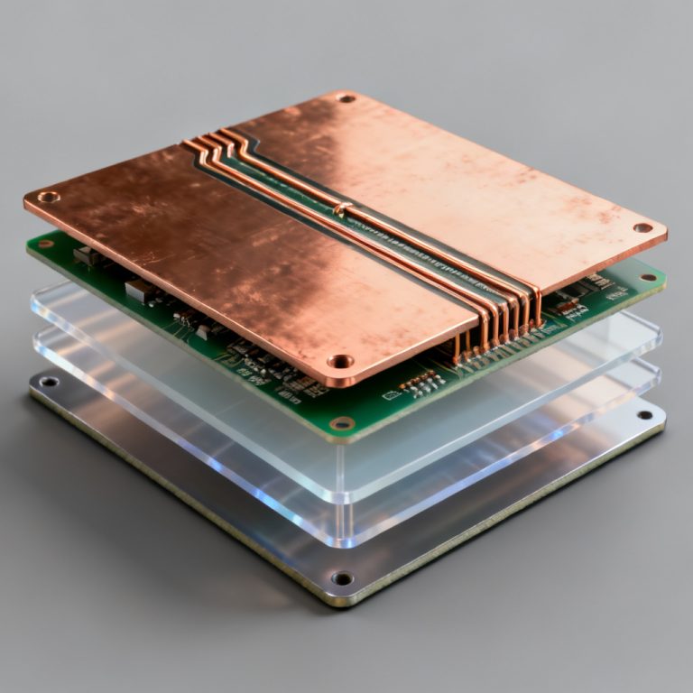
The foundation of impedance control is the stackup. For BGA breakout, the distance between the signal layer and its adjacent reference plane (ground or power) must be carefully chosen.
- Thin Dielectrics for Inner Layers: For stripline routing (signals sandwiched between two planes), use very thin dielectric cores (e.g., 3-4 mils prepreg or core). This allows narrow traces (4-5 mils) to achieve 50-ohm impedance. Thinner dielectrics also reduce crosstalk between adjacent traces.
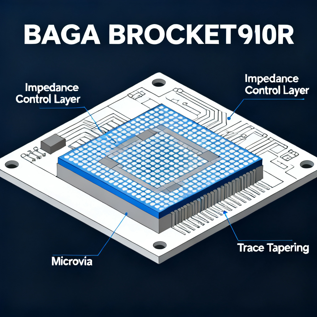
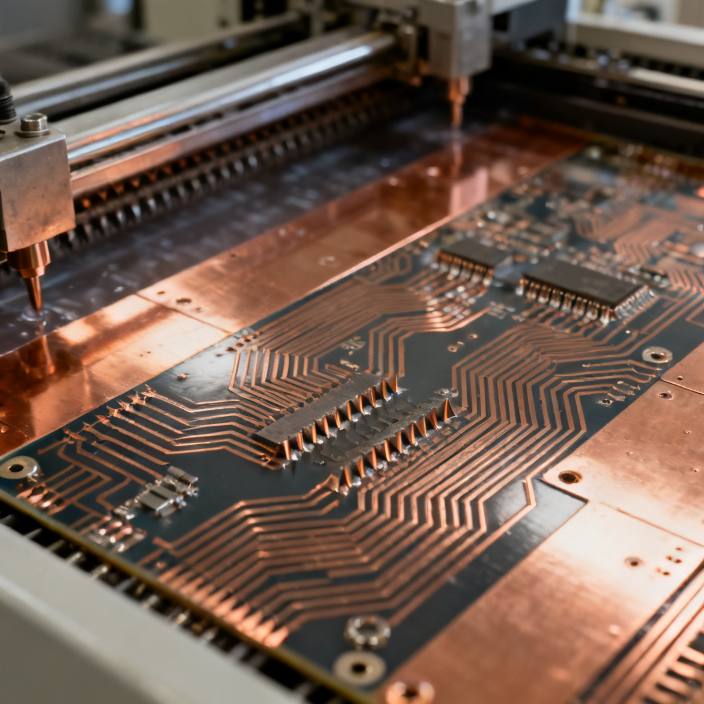
- Use of High-Density Interconnect (HDI) Structures: For ultra-fine pitch BGAs (< 0.8mm), traditional through-hole vias are too large. HDI technology with microvias (laser-drilled, typically 4-6 mils in diameter) is essential. Use a sequential build-up (SBU) structure: a core layer with through-holes, followed by one or more layers of microvias on each side.
- Reference Plane Proximity: Ensure that every signal layer in the breakout region has an uninterrupted reference plane directly adjacent (within 3-5 mils). Avoid splitting the plane under the BGA. If a power plane is used, ensure it is AC-coupled to ground with decoupling capacitors.
2.2 Trace Geometry: Width, Spacing, and Tapering
The most common cause of impedance mismatch in BGA breakout is the abrupt change in trace width.
- Trace Width Calculation: Use an impedance calculator (e.g., Polar Si9000) to determine the exact trace width needed for your target impedance (usually 50 ohms single-ended or 100 ohms differential) given your specific stackup. For the breakout region, this width will be the “bottleneck” width.
- Tapered Transitions: Do not simply step the trace from a narrow width (inside BGA) to a wide width (outside). Instead, use a tapered transition (a gradual widening of the trace over a length of 10-20 mils). This reduces the impedance discontinuity. The taper should be smooth and symmetrical.
- Dogbone vs. Direct Connect: For BGA pads, use a “dogbone” pattern where a small pad is connected to a short, narrow trace. Avoid connecting a wide trace directly to the BGA pad, as the pad’s capacitance will lower the impedance locally. The dogbone trace should be the same width as the breakout trace.
2.3 Via Management: Microvias, Stub Reduction, and Anti-Pads
Vias are notorious impedance disruptors. In BGA breakout areas, they are unavoidable.
- Microvias Instead of Through-Holes: For signals that need to change layers under the BGA, use stacked or staggered microvias. Microvias have much lower parasitic capacitance and inductance than through-holes. They also allow for tighter routing channels.
- Via Stub Reduction: A through-hole via that extends beyond the target layer creates a “stub” that acts as a resonant cavity, causing reflections at high frequencies. Back-drilling (drilling out the unused portion of the via) is critical for signals above 5 GHz. Alternatively, use buried vias (connecting only inner layers) to eliminate stubs entirely.
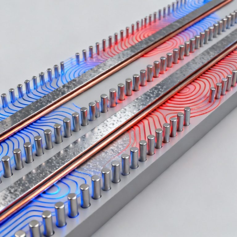
- Optimized Anti-Pad Size: The anti-pad (the clearance hole in the reference plane around the via) must be carefully sized. A small anti-pad increases capacitance, lowering impedance. A large anti-pad increases inductance, raising impedance. The optimal anti-pad diameter is typically 2x to 3x the via pad diameter. Use a grounded via (a via connecting the reference planes) near each signal via to provide a low-inductance return path.
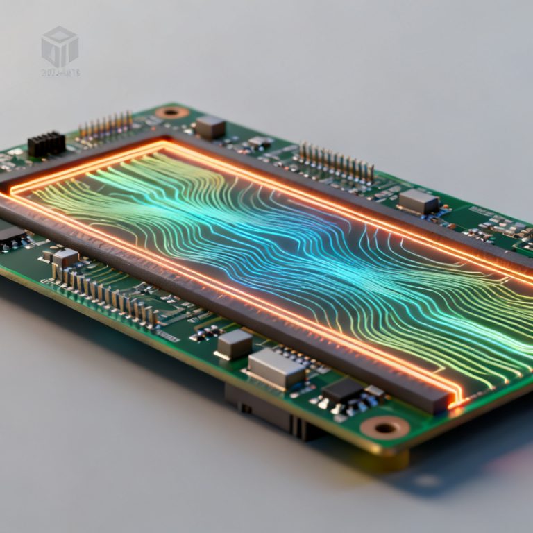
- Via Fencing: For high-speed differential pairs (e.g., PCIe, USB 3.0), place ground vias on either side of the pair, forming a “fence.” This confines the electromagnetic field and reduces crosstalk between pairs.
2.4 Differential Pair Routing in BGA Breakout
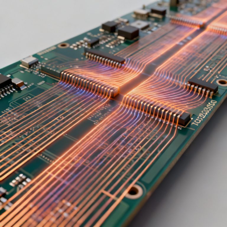
Differential pairs (e.g., for high-speed serial links) require even tighter control.
- Intra-Pair Skew: The two traces of a differential pair must be exactly equal in length. In BGA breakout, this is achieved by using symmetric routing. If one trace needs to go around a via or pad, the other trace must have a matching “serpentine” delay.
- Coupling Consistency: Maintain a constant edge-to-edge spacing between the two traces of a pair. In the breakout region, this spacing is often forced to be very small (e.g., 4-5 mils). Outside the BGA, maintain this same spacing. Do not spread the pair apart to meet a wider trace width requirement; instead, use a thinner dielectric to achieve the target differential impedance.
- Return Path: For differential pairs, the return current flows in the adjacent reference plane. Ensure this plane is continuous and has no splits under the breakout area.
Section 3: Material Selection for High-Speed BGA Breakout
The choice of PCB laminate material is a critical factor in achieving consistent impedance, especially at high frequencies. The key material properties are the dielectric constant (Dk) and the dissipation factor (Df).
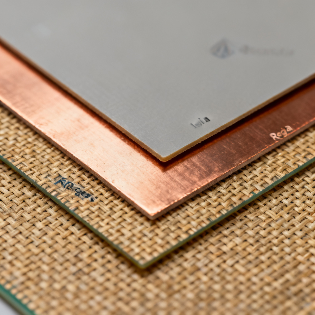
- Dk Tolerance: Standard FR-4 has a Dk of 4.2-4.5, but its tolerance is poor (+/- 10-15%). For controlled impedance, you need materials with tight Dk tolerance (+/- 2-3%). Examples include Isola 370HR (Dk 4.1, Df 0.015) or Rogers 4350B (Dk 3.48, Df 0.0037).
- Low Df for High Frequencies: For signals above 5 GHz, the Df (loss tangent) becomes critical. FR-4 has a high Df (0.02-0.03), causing significant signal loss. Use low-loss materials like Rogers 4000 series or Panasonic Megtron 6 (Df < 0.005).
- Resin Content and Glass Weave: The glass weave in the laminate can cause local variations in Dk (called “fiber weave effect”). For very high-speed designs (e.g., 25+ Gbps), use spread-glass or flat-glass laminates (e.g., Rogers 4350B with 1080 glass) to minimize this effect. Alternatively, rotate the traces by 10-15 degrees relative to the weave direction.
- Material Compatibility: If using a hybrid stackup (e.g., FR-4 core with Rogers outer layers), ensure the materials have compatible coefficients of thermal expansion (CTE) to prevent delamination during assembly.
Section 4: Manufacturing Considerations for Impedance Consistency
Even the best design can fail if the manufacturing process is not carefully controlled. Here are the critical manufacturing parameters that affect impedance in BGA breakout areas.
4.1 Etching and Trace Profile
- Etch Factor: The etching process removes copper from the sides of the trace, creating a trapezoidal cross-section. The “etch factor” (ratio of vertical etch to lateral etch) determines the final trace width at the bottom vs. the top. For controlled impedance, the trace width must be measured at the top of the trace (the widest point). Work with your fabricator to ensure a consistent etch factor.
- Under-Cut: Excessive under-cut (lateral etching) will make the trace narrower than designed, increasing its impedance. Use a positive etch factor (more vertical than lateral) for best results.
4.2 Prepreg and Core Thickness Tolerance
- Dielectric Thickness: The actual thickness of the prepreg or core after lamination can vary by +/- 10% from the nominal value. This directly affects impedance. Use a fabricator with tight process control (e.g., +/- 5% tolerance). Specify “controlled impedance” on the fabrication drawing, and provide the target impedance values.
- Resin Flow: During lamination, the resin in the prepreg flows, potentially thinning the dielectric near the edges of the board. This is less of an issue in the BGA area (which is usually in the center of the board), but it can affect impedance if the breakout extends to the board edge.
4.3 Solder Mask Influence
- Solder Mask Thickness: The solder mask has a dielectric constant (typically 3.5-4.0) that is lower than the core material. When applied over a microstrip trace, it lowers the impedance (by increasing the effective dielectric thickness). For very thin traces (e.g., 4 mils), the solder mask can reduce impedance by 2-4 ohms.
- Solution: Either account for the solder mask in your impedance calculations (using a “solder mask on” model) or request that the fabricator leave the breakout area un-masked (solder mask defined only on the pads). For high-volume production, the latter is often preferred.
4.4 Surface Finish
- ENIG vs. HASL: Electroless Nickel Immersion Gold (ENIG) is preferred over Hot Air Solder Leveling (HASL) for fine-pitch BGAs because it provides a flat surface. However, the nickel layer in ENIG has a different resistivity than copper, which can affect impedance at very high frequencies (above 10 GHz). For such designs, consider Immersion Silver or OSP (Organic Solderability Preservative).
Section 5: Verification and Testing
After manufacturing, it is essential to verify that the impedance targets have been met.
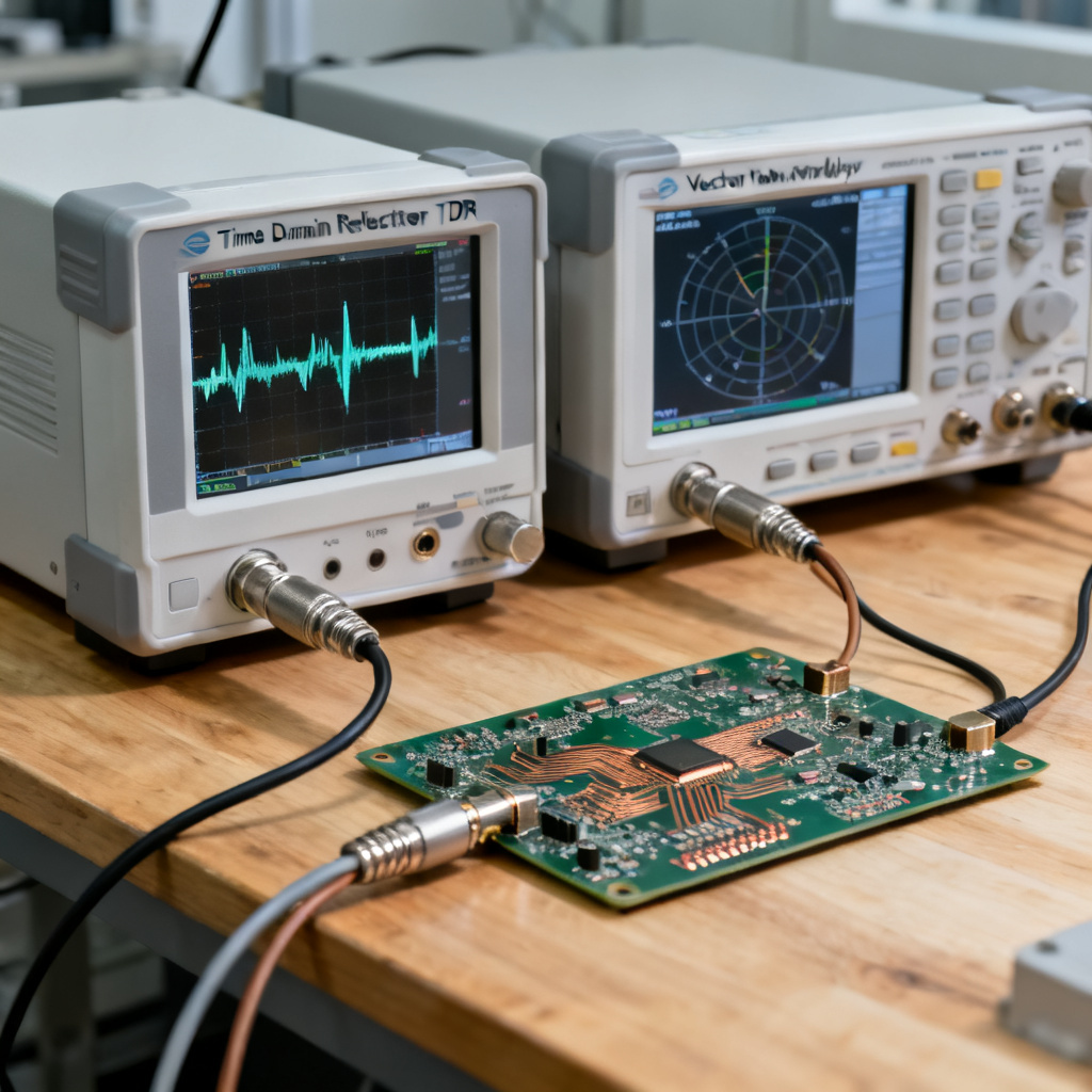
- Time Domain Reflectometry (TDR): A TDR sends a fast pulse down the trace and measures the reflections. This can pinpoint the exact location of impedance discontinuities (e.g., at the BGA pad, at the via, or at the trace width transition). Use TDR to validate the breakout area.
- Coupon Testing: Most fabricators include impedance test coupons on the panel. These are dedicated test structures that mimic the trace geometry in the breakout area. Ensure the coupons are representative of the actual routing.
- Vector Network Analyzer (VNA): For very high-frequency designs (above 10 GHz), use a VNA to measure the S-parameters (return loss, insertion loss) of the breakout path. A return loss better than -15 dB is typical for a well-designed breakout.
Comparison: Standard vs. Optimized Impedance Control PCB for BGA Breakout
| Parameter | Standard Approach | Optimized Impedance Control PCB for BGA Breakout |
|---|---|---|
| Dielectric Thickness | 4-5 mils (variable) | 3-4 mils (tight tolerance) |
| Trace Width Consistency | Abrupt changes | Tapered transitions |
| Via Type | Through-hole | Microvia + back-drilling |
| Material Dk Tolerance | +/- 10% | +/- 2% |
| Impedance Variation | +/- 15% | +/- 5% |
FAQ: Impedance Control PCB for BGA Breakout
What is impedance control PCB for BGA breakout?
Impedance control PCB for BGA breakout refers to the design and manufacturing techniques used to maintain a consistent characteristic impedance for traces routing from a Ball Grid Array package, especially in dense areas where trace width and spacing are constrained.
Why is impedance consistency critical in BGA breakout?
Impedance consistency prevents signal reflections, reduces jitter, and ensures high-speed digital signals maintain integrity. In dense BGA areas, even small discontinuities can cause data errors or system failure.
What materials are best for impedance control PCB for BGA breakout?
Low-loss materials with tight Dk tolerance such as Rogers 4350B, Isola 370HR, or Panasonic Megtron 6 are recommended. These materials minimize impedance variation and signal loss at high frequencies.
How do microvias improve impedance control in BGA breakout?
Microvias have lower parasitic capacitance and inductance than through-hole vias, reducing impedance discontinuity. They also allow tighter routing channels and shorter stub lengths.
Can solder mask affect impedance in BGA breakout?
Yes, solder mask can lower impedance by 2-4 ohms on thin traces. Designers should either account for it in calculations or request unmasked breakout areas.