In high-speed PCB design, the power delivery network (PDN) is often the unsung hero—or the silent saboteur. Power supply induced jitter is one of the most critical and often misunderstood phenomena, where ripple on the PDN couples into voltage-controlled oscillators (VCOs) or clock buffers, causing timing uncertainty that degrades system margin. This pillar content synthesizes the most authoritative knowledge from industry leaders to provide an exhaustive understanding of how PDN ripple translates into jitter, how to model it, and how to mitigate it in your high-speed PCB designs.
The Fundamental Mechanism – How PDN Ripple Becomes Power Supply Induced Jitter
The Core Physics: Voltage Sensitivity of Timing Elements
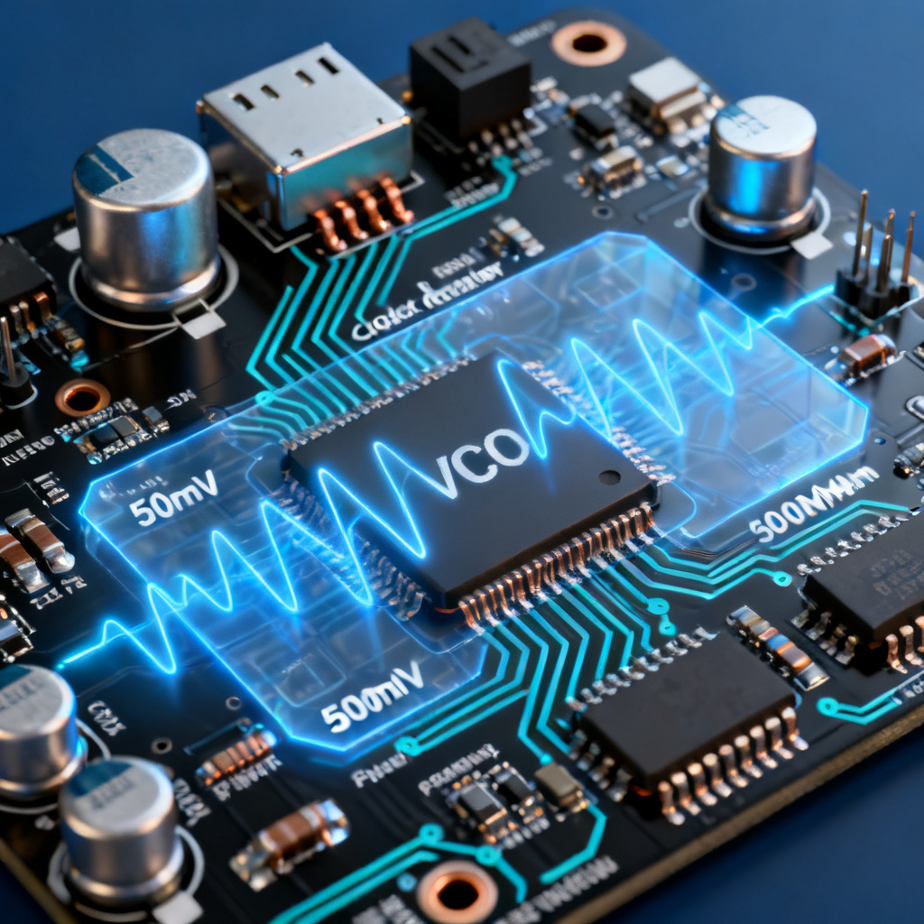
At the heart of power supply induced jitter is the voltage-to-frequency sensitivity of active components. A VCO’s output frequency is directly controlled by its input voltage. Similarly, a clock buffer’s propagation delay varies with its supply voltage due to changes in transistor switching speed. When the PDN contains ripple—periodic or random voltage fluctuations—these variations modulate the instantaneous frequency or delay, creating jitter.
Key Insight from Industry Research: The transfer function from PDN ripple to output jitter is not linear in all cases. It depends on the device’s power supply rejection ratio (PSRR) at specific frequencies. PSRR quantifies how much a device attenuates supply noise before it reaches the output. For a VCO, PSRR is often frequency-dependent: low-frequency ripple (e.g., 50/60 Hz or switching regulator ripple) may be well-rejected, but ripple near the VCO’s control loop bandwidth can cause significant jitter.
The Role of PDN Impedance and Resonances
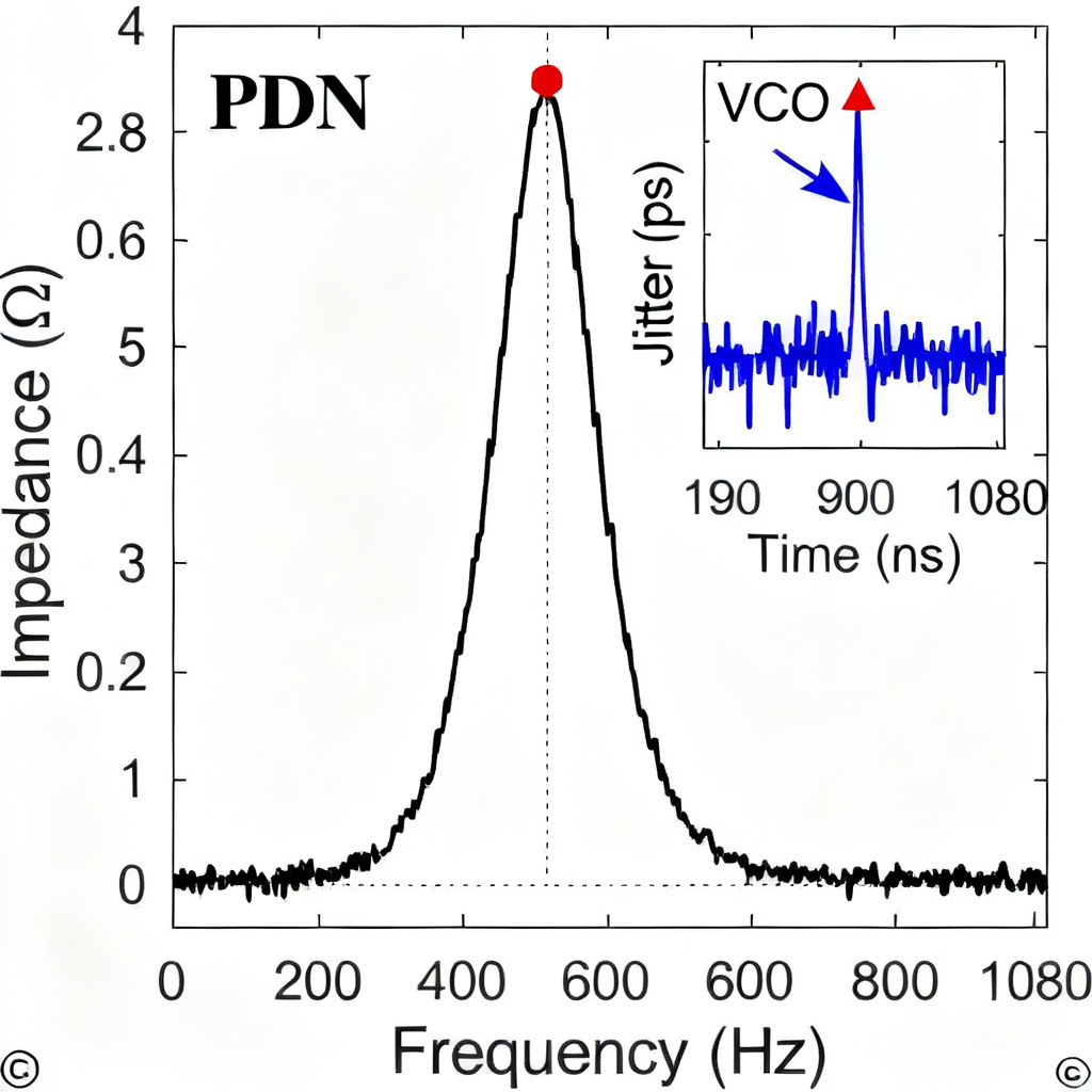
A poorly designed PDN exhibits impedance peaks at specific frequencies, typically caused by the anti-resonance between decoupling capacitors and the PCB’s intrinsic inductance. These peaks amplify ripple at those frequencies. When a VCO or buffer operates near such a resonance, the jitter impact multiplies.
Critical Point from Expert Analysis: The relationship between PDN impedance and jitter is captured by the jitter sensitivity function (often denoted as K_v for VCOs or K_b for buffers). This function, usually provided by component datasheets or derived through simulation, converts a given voltage ripple amplitude (in mV) at a specific frequency into output jitter (in ps). For example, a 10 mV ripple at 1 MHz might cause 0.5 ps of jitter in a buffer, while the same ripple at 100 MHz might cause 5 ps.
The Difference Between VCO and Buffer PSIJ
While both VCOs and buffers are susceptible, their mechanisms differ:
- VCO: The frequency modulation is direct. Ripple on the control voltage (or supply for ring oscillators) changes the oscillation frequency. This results in periodic jitter (PJ) at the ripple frequency and its harmonics.
- Buffer: Ripple changes the transistor’s saturation current and threshold voltage, altering the propagation delay. This can cause both periodic jitter (if ripple is periodic) and random jitter (if ripple is broadband noise). The buffer’s PSRR is typically better at low frequencies but degrades at higher frequencies due to reduced feedback loop gain.
Modeling and Simulation – From PDN Ripple to Power Supply Induced Jitter
The Complete Chain: PDN → Device → Jitter
To accurately predict power supply induced jitter, designers must model the entire chain:
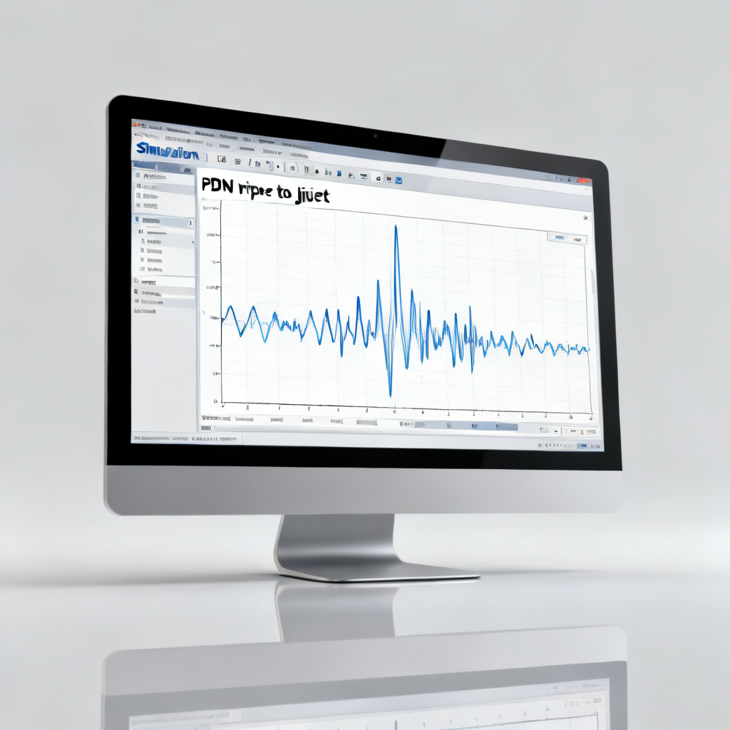
- PDN Impedance Profile: Simulate or measure the PDN impedance from the power source to the VCO/buffer’s power pin. Use tools like SIwave, PowerSI, or CST to capture resonances up to the device’s bandwidth.
- Ripple Source Characterization: Identify all ripple sources: switching regulators (fundamental and harmonics), digital switching noise, and external interference. Convert these into voltage noise spectra at the device pin.
- Device Jitter Sensitivity: Obtain the jitter sensitivity curve from the datasheet or through SPICE simulation. For VCOs, this is often
K_v(MHz/V). For buffers, it’s a delay sensitivity (ps/mV) vs. frequency. - Convolution: Multiply the ripple spectrum by the sensitivity function to get the jitter spectrum. The total jitter is the root-sum-square (RSS) of all components.
Advanced Modeling Techniques from Industry Leaders
- S-Parameter Based PDN Models: Use S-parameters for the PDN to capture frequency-dependent behavior accurately. This is superior to lumped-element models for high-frequency resonances.
- Behavioral Jitter Models: For complex devices, use behavioral models (e.g., Verilog-A) that incorporate PSRR and jitter sensitivity. These allow co-simulation with the PDN.
- Transient Noise Analysis: In time-domain simulations, inject a realistic ripple waveform (e.g., from a switching regulator model) at the device supply and measure the output jitter directly. This is the most accurate but computationally expensive.
A Practical Example: 10 mV Ripple at 1 MHz
Assume a clock buffer with a jitter sensitivity of 1 ps/mV at 1 MHz (typical for a high-speed LVDS buffer). A 10 mV peak-to-peak ripple at 1 MHz will cause:
- Periodic Jitter (PJ) = Sensitivity × Ripple Amplitude = 1 ps/mV × 10 mV = 10 ps (peak-to-peak).
- This jitter appears as a deterministic component in the eye diagram, reducing the eye opening by 10 ps.
If the same ripple occurs at 100 MHz, and the buffer’s PSRR degrades (sensitivity = 5 ps/mV), the jitter becomes 50 ps, which could be catastrophic for a 10 Gbps link (100 ps unit interval).
Mitigation Strategies – Designing for Low Power Supply Induced Jitter
PDN Design Best Practices
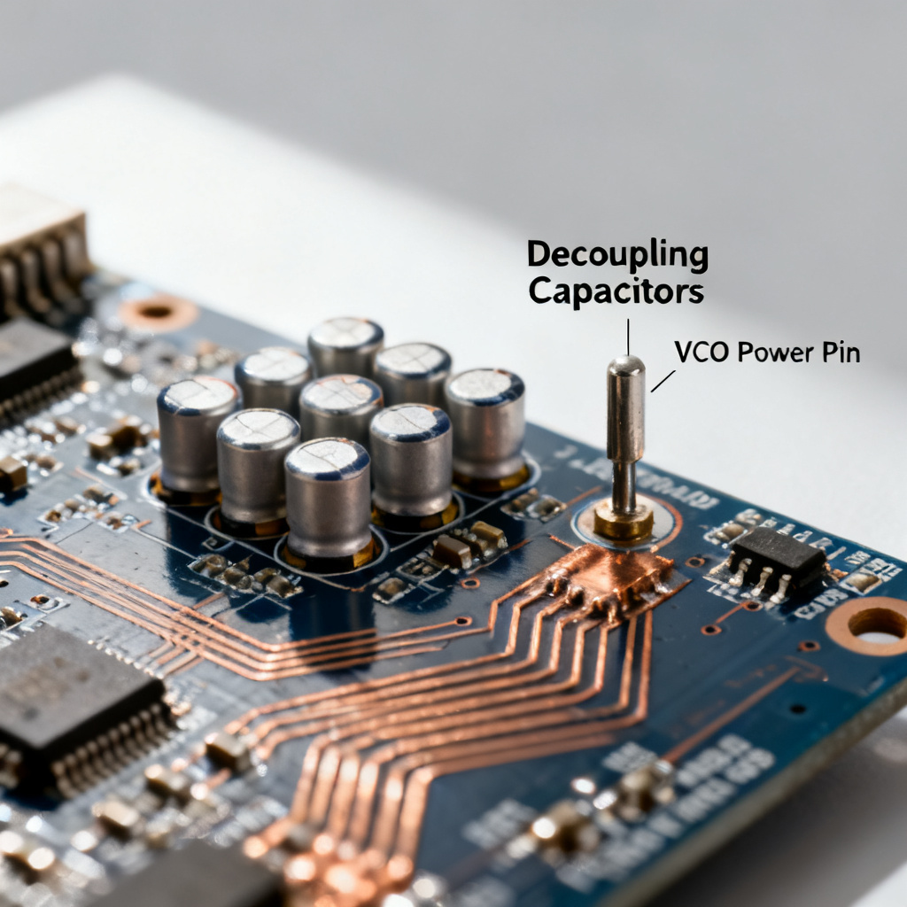
- Target Impedance: Design the PDN to have a flat, low impedance (e.g., < 0.1 ohm) across all frequencies where the device is sensitive. Use multiple decoupling capacitor values (e.g., 100 nF, 10 nF, 1 nF, 100 pF) to cover a wide frequency range.
- Avoid Anti-Resonance: Place capacitors with overlapping impedance curves. Use a combination of bulk electrolytic, ceramic, and low-ESL capacitors. Simulate the PDN to ensure no impedance peaks exceed the target.
- Localized Decoupling: Place the smallest capacitors (e.g., 100 pF) as close as possible to the VCO/buffer power pin. This minimizes trace inductance and provides the highest frequency decoupling.
Component Selection and Layout
- Use High-PSRR Devices: Select VCOs and buffers with high PSRR at the frequencies of concern. For example, a PLL-based clock cleaner may have >60 dB PSRR at 1 MHz but only 20 dB at 100 MHz.
- Isolate Sensitive Power Domains: Use dedicated power planes or islands for VCOs and clock buffers. Do not share them with noisy digital logic or I/O buffers.
- Guard Rings and Grounding: Surround VCO/buffer power pins with ground vias to create a low-inductance return path. Use guard rings on the PCB to prevent noise coupling from adjacent traces.
Filtering and Regulation
- Low-Noise LDOs: Use low-dropout regulators (LDOs) with high PSRR (e.g., >70 dB up to 1 MHz) to power VCOs and buffers. LDOs can attenuate ripple from switching regulators.
- Ferrite Beads and Pi Filters: Add ferrite beads in series with the power trace to suppress high-frequency noise. Combine with capacitors to form a Pi filter (C-L-C) for maximum attenuation.
- Switching Regulator Optimization: If using a switching regulator, choose one with spread-spectrum modulation to reduce peak ripple amplitude. Keep the switching frequency away from the VCO/buffer’s sensitive frequencies.
Post-Layout Verification
- Measure PDN Impedance: Use a vector network analyzer (VNA) to measure the PDN impedance at the device power pin. Compare with simulation.
- Jitter Measurement: Use a real-time oscilloscope or jitter analyzer to measure the output jitter of the VCO/buffer under actual operating conditions. Correlate with PDN ripple measurements.
- Iterate and Optimize: If jitter exceeds the budget, identify the dominant ripple frequency and add targeted filtering or change the decoupling capacitor values.
Real-World Case Studies and Lessons Learned
Case Study 1: 10 Gbps SerDes Jitter Failure
Problem: A 10 Gbps SerDes link showed excessive jitter (30 ps peak-to-peak) on the recovered clock, causing bit errors. The VCO was powered by a 1.8V supply derived from a buck converter.
Analysis: The PDN impedance showed a 2-ohm peak at 2.2 MHz, exactly the switching frequency of the buck converter. The VCO’s jitter sensitivity at 2.2 MHz was 3 ps/mV. The ripple amplitude at the VCO pin was 15 mV peak-to-peak.
Solution: Added a 10 µF capacitor in parallel with the existing 1 µF capacitor to lower the PDN impedance at 2.2 MHz. Also added a ferrite bead (100 MHz impedance = 600 ohms) in series with the power trace. Post-fix jitter reduced to 5 ps.
Lesson: A single impedance peak can cause catastrophic jitter. Always simulate the PDN at the switching regulator frequency.
Case Study 2: Clock Buffer Jitter from Digital Switching Noise
Problem: A 156.25 MHz clock buffer exhibited 8 ps of random jitter, degrading the timing margin of a 10 GbE PHY.
Analysis: The buffer shared a power plane with a high-speed FPGA. The FPGA’s core switching noise created broadband ripple from 10 MHz to 1 GHz. The buffer’s PSRR was only 20 dB above 100 MHz.
Solution: Moved the buffer to a separate power island with a dedicated LDO (PSRR = 70 dB at 100 MHz). Added a 100 pF capacitor directly at the buffer pin. Jitter dropped to 2 ps.
Lesson: Sharing power planes with noisy digital logic is a common mistake. Isolate sensitive analog/clock components.
Case Study 3: VCO Phase Noise Degradation
Problem: A 5 GHz VCO used in a phase-locked loop showed increased phase noise at 100 kHz offset, causing poor EVM in a 64-QAM system.
Analysis: The PDN had a resonance at 100 kHz due to the interaction of a bulk capacitor (100 µF) and the PCB’s plane inductance. The 100 kHz ripple modulated the VCO frequency, creating phase noise sidebands.
Solution: Added a 1 µF capacitor in parallel with the 100 µF to shift the resonance frequency. Also used a low-noise LDO with >80 dB PSRR at 100 kHz. Phase noise improved by 10 dB.
Lesson: Low-frequency resonances can be just as damaging as high-frequency ones, especially for VCOs with narrow loop bandwidths.
Integration into Your High-Speed PCB Design Flow
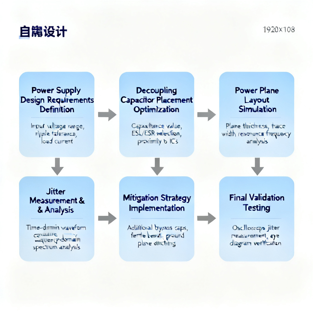
Design Checklist for PSIJ Mitigation
- [ ] Identify all VCOs and clock buffers in the design.
- [ ] Obtain jitter sensitivity curves from datasheets or simulation.
- [ ] Simulate PDN impedance from source to each sensitive device.
- [ ] Identify all ripple sources (regulators, digital noise, external).
- [ ] Calculate expected jitter using convolution method.
- [ ] If jitter exceeds budget, iterate on decoupling, isolation, or component selection.
- [ ] Verify with post-layout PDN measurement and jitter measurement.
Tools and Resources
| Tool/Resource | Purpose for Power Supply Induced Jitter Analysis |
|---|---|
| Ansys SIwave | PDN impedance simulation and ripple analysis |
| Cadence Sigrity | Power integrity and jitter sensitivity modeling |
| Keysight ADS | Co-simulation of PDN and jitter |
| CST Studio Suite | 3D EM simulation for PDN resonances |
| VNA | PDN impedance measurement |
| Real-time oscilloscope | Jitter measurement and ripple characterization |
| Spectrum analyzer | Ripple frequency domain analysis |
When to Call a Specialist
If your design involves:
- Data rates > 10 Gbps
- Multi-gigahertz VCOs
- Mixed-signal systems with high-power digital and sensitive analog
- Tight jitter budgets (< 1 ps)
Consider engaging a signal/power integrity consultant or using advanced simulation services.
Frequently Asked Questions (FAQ) About Power Supply Induced Jitter
What is power supply induced jitter in high-speed PCB design?
Power supply induced jitter is timing uncertainty caused by ripple on the power delivery network (PDN) that modulates the output frequency or delay of voltage-controlled oscillators (VCOs) or clock buffers, directly impacting signal integrity.
How does PDN ripple cause jitter in VCOs?
PDN ripple changes the VCO’s control voltage or supply voltage, which alters its oscillation frequency. This frequency modulation results in periodic jitter at the ripple frequency and its harmonics.
What is the role of PSRR in power supply induced jitter?
Power supply rejection ratio (PSRR) quantifies how much a device attenuates supply noise. High PSRR at the ripple frequency reduces the amount of jitter induced, making it a key parameter for selecting components.
How can I mitigate power supply induced jitter in my PCB?
Mitigation strategies include designing a low-impedance PDN, using localized decoupling, selecting high-PSRR components, isolating sensitive power domains, and employing low-noise LDOs or ferrite bead filters.
What tools are used to simulate power supply induced jitter?
Common tools include Ansys SIwave, Cadence Sigrity, Keysight ADS, and CST Studio Suite. These tools enable PDN impedance simulation, ripple characterization, and jitter sensitivity analysis.