In high-speed PCB design, the integrity of the clock signal is paramount. As data rates push into the multi-gigabit range, even picoseconds of jitter can cause bit errors, link failures, and system instability. The Phase Locked Loop Jitter in High Speed PCB is the cornerstone of clock management, performing two critical functions: reference clock cleanup (filtering noise from an incoming clock) and clock multiplication (generating higher-frequency clocks from a lower-frequency reference). This pillar page integrates the most authoritative knowledge from industry leaders to provide a definitive guide on PLL jitter, its sources, measurement, and mitigation in high-speed PCB applications.
1. Understanding PLL Basics and Jitter Fundamentals in High Speed PCB
1.1 What is a PLL and Why Does It Matter in High Speed PCB?
A Phase-Locked Loop is a feedback control system that synchronizes an output oscillator signal with a reference input signal in both frequency and phase. In high-speed PCBs, PLLs are embedded in FPGAs, SERDES transceivers, clock generators, and jitter cleaners. Their primary roles are:
– Reference Clock Cleanup: Removing high-frequency jitter (phase noise) from a noisy reference clock (e.g., from a crystal oscillator or backplane) to produce a clean, stable clock for sensitive circuits.
– Clock Multiplication: Generating a high-frequency clock (e.g., 10 GHz) from a lower-frequency reference (e.g., 100 MHz) using the PLL’s voltage-controlled oscillator (VCO) and feedback divider.
1.2 Types of Jitter in PLL Systems for High Speed PCB
Jitter is the deviation of a clock edge from its ideal position. In PLL contexts, it is categorized into:
– Random Jitter (RJ): Unbounded, Gaussian-distributed jitter caused by thermal noise, shot noise, and flicker noise in the PLL components (phase detector, charge pump, VCO). It accumulates over time and is quantified by its RMS value.
– Deterministic Jitter (DJ): Bounded, predictable jitter from systematic sources like power supply noise, crosstalk, and electromagnetic interference (EMI). DJ includes:
– Periodic Jitter (PJ): Sinusoidal jitter from switching regulators or clock harmonics.
– Data-Dependent Jitter (DDJ): Correlated with the data pattern, often from intersymbol interference (ISI).
– Duty-Cycle Distortion (DCD): Unequal high/low times in the clock.
– Total Jitter (TJ): The sum of RJ and DJ, often specified at a bit error rate (BER) of \(10^{-12}\) in high-speed serial links.
1.3 Phase Noise vs. Jitter in High Speed PCB
Phase noise is the frequency-domain representation of jitter, measured in dBc/Hz at specific offsets from the carrier. Jitter is the time-domain equivalent. The relationship is:
\[
\text{Jitter (RMS)} = \frac{1}{2\pi f_c} \sqrt{2 \int_{f_1}^{f_2} 10^{\frac{L(f)}{10}} df}
\]
where \(f_c\) is the carrier frequency, and \(L(f)\) is the single-sideband phase noise. For PLL design, phase noise at low offsets (1 kHz–100 kHz) determines long-term jitter, while high-offset noise (1 MHz–100 MHz) affects short-term jitter.
2. PLL Architecture and Jitter Sources in High Speed PCB
2.1 Core PLL Components and Their Jitter Contributions in High Speed PCB
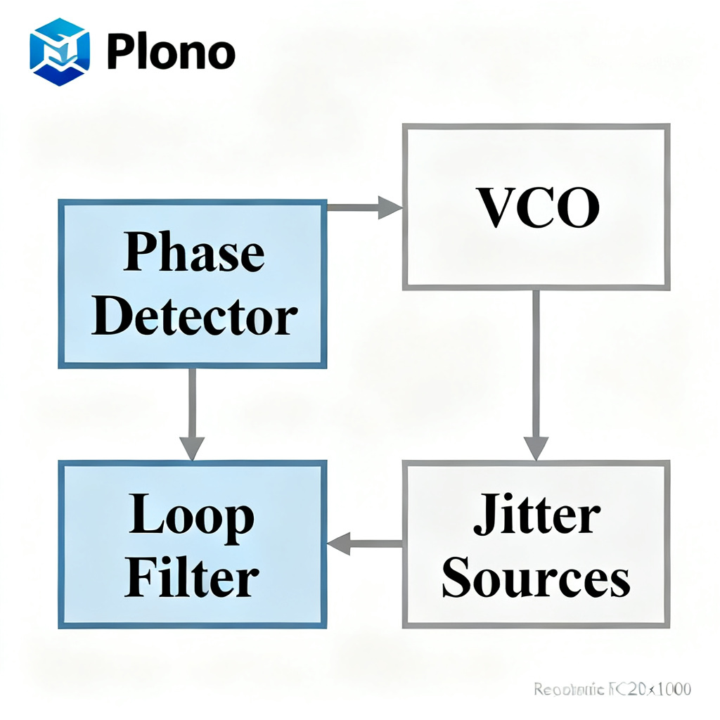
A typical PLL consists of:
– Phase Frequency Detector (PFD): Compares the reference and feedback clocks. Dead-zone issues can introduce DJ if the phase error is too small.
– Charge Pump (CP): Converts the PFD output into a current. Mismatches between up/down currents cause static phase offset and jitter.
– Loop Filter (LF): A low-pass filter (usually RC or active) that sets the PLL bandwidth. It filters out high-frequency noise from the PFD/CP but cannot suppress VCO noise.
– Voltage-Controlled Oscillator (VCO): The dominant jitter source. Its phase noise is shaped by the loop bandwidth. LC oscillators have lower noise than ring oscillators but consume more area.
– Feedback Divider (N): Multiplies the reference frequency. A higher N factor amplifies the reference noise and PFD/CP noise by \(20 \log(N)\) dB.
2.2 Jitter Transfer, Jitter Generation, and Jitter Tolerance in High Speed PCB
These three PLL metrics are critical for high-speed links:
– Jitter Transfer: How the PLL attenuates jitter on the reference clock. A low loop bandwidth (e.g., 1 MHz) provides better jitter filtering but slower lock time.
– Jitter Generation: The jitter the PLL adds internally. This is dominated by the VCO and power supply noise.
– Jitter Tolerance: The ability of the PLL to track input jitter without losing lock. High bandwidth improves tolerance but degrades cleanup.
2.3 Reference Clock Cleanup: How PLLs Filter Jitter in High Speed PCB
A PLL acts as a high-pass filter for its own VCO noise and a low-pass filter for the reference noise. For clock cleanup:
– Narrow Bandwidth (e.g., 100 kHz): Excellent rejection of reference jitter and PFD/CP noise. The output jitter is dominated by the VCO’s close-in phase noise.
– Trade-off: Narrow bandwidth increases lock time and makes the PLL sensitive to VCO drift and temperature changes.
– Best Practice: Use a PLL with a programmable bandwidth and select a value that aligns with the reference’s noise profile. For example, if the reference has high jitter above 1 MHz, set the loop bandwidth below 1 MHz.
2.4 Clock Multiplication: Jitter Amplification Mechanisms in High Speed PCB
When multiplying a reference clock (e.g., 100 MHz to 10 GHz, N=100):
– Reference Noise Amplification: The jitter on the reference is multiplied by N. If the reference has 1 ps RMS jitter, the output will have ~100 ps RMS jitter from this source alone.
– PFD/CP Noise: These are also amplified by N. A low-noise PFD/CP is essential.
– VCO Noise: Not multiplied by N, but shaped by the loop. A low-noise VCO (e.g., LC-based) is critical.
– Fractional-N PLLs: Introduce quantization noise from the delta-sigma modulator, which can be filtered by the loop but may cause spurious tones.
3. Jitter Measurement and Characterization for High Speed PCB
3.1 Time-Domain Measurement Techniques for High Speed PCB Jitter
– Oscilloscope (Real-Time or Sampling):
– Measures TIE (Time Interval Error), period jitter, and cycle-to-cycle jitter.
– For high-frequency PLL outputs (e.g., 10 GHz), use a sampling oscilloscope with a low-jitter trigger.
– Limitation: Oscilloscope noise floor (typically 200–500 fs RMS) can mask low-jitter signals.
– BER Tester (BERT):
– Measures TJ at a specific BER (e.g., \(10^{-12}\)) by scanning a variable delay.
– Provides the most accurate TJ for serial links.
– Time Interval Analyzer (TIA):
– Captures long sequences of clock edges for jitter histogram and spectrum analysis.
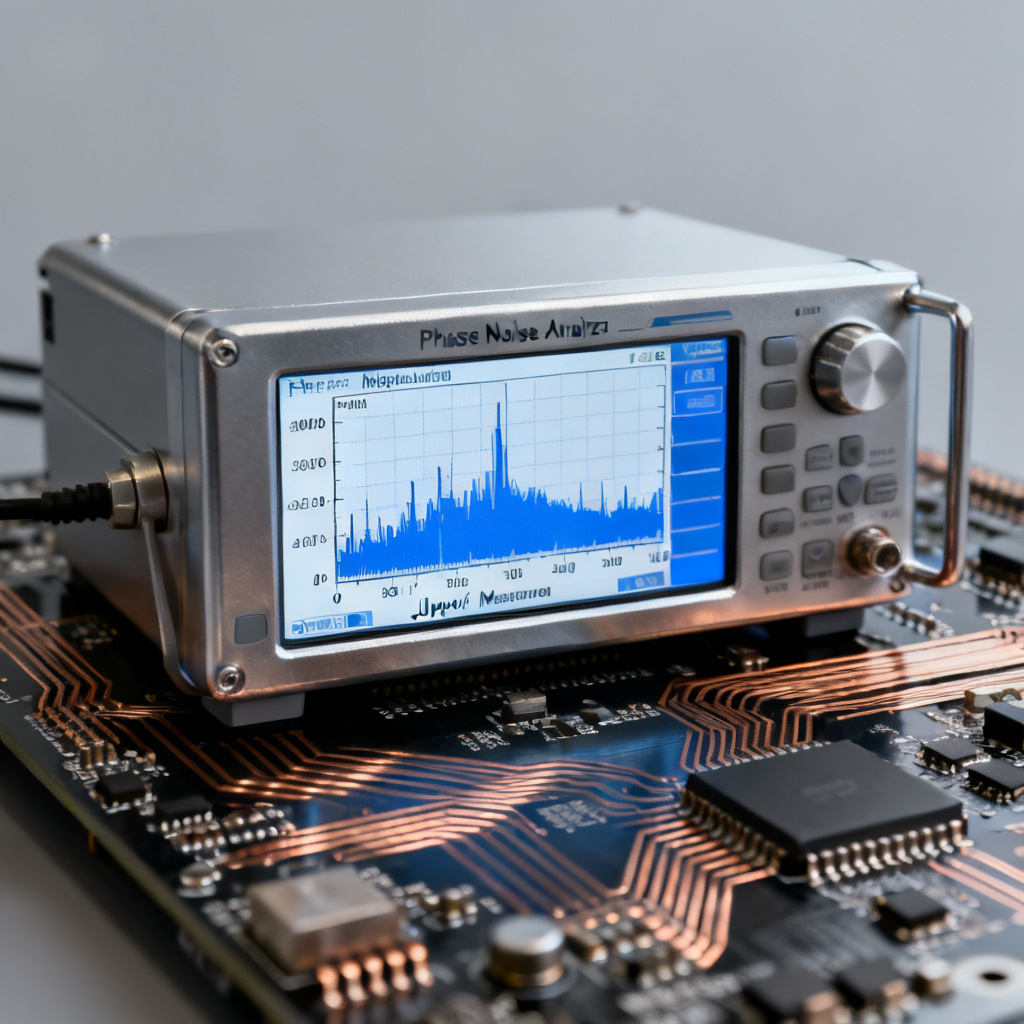
3.2 Frequency-Domain Phase Noise Measurement for High Speed PCB
– Phase Noise Analyzer (e.g., Keysight E5052B, Rohde & Schwarz FSWP):
– Measures phase noise from 1 Hz to 100 MHz offsets.
– Integrate phase noise over the relevant bandwidth (e.g., 12 kHz to 20 MHz for PCIe Gen 5) to compute RMS jitter.
– Cross-Correlation Method: Used for ultra-low-noise PLLs (< 100 fs RMS). Two analyzers cross-correlate to cancel internal noise. – Spurious Signals: Identify deterministic jitter from power supply harmonics (e.g., 50/60 Hz and switching frequency).
3.3 Key Jitter Specifications for High-Speed Standards in High Speed PCB
– PCIe Gen 5/6: Total jitter at BER \(10^{-12}\) < 0.5 ps RMS for the reference clock (100 MHz). – 100GbE (CAUI-4): Phase noise integration from 10 kHz to 10 MHz < 100 fs RMS. – JEDEC JESD204B/C: Clock jitter < 200 fs RMS for 12+ bit ADCs. – SERDES (e.g., Xilinx GTH/GTY): Input reference clock jitter < 1 ps RMS typical.
4. Practical PCB Design Strategies for Minimizing PLL Jitter in High Speed PCB
4.1 Power Supply Integrity (PSI) for High Speed PCB
Power supply noise is the #1 cause of deterministic jitter in PLLs.
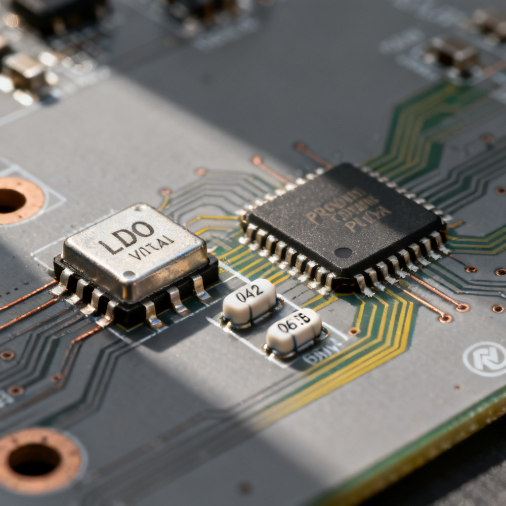
– Use Low-Noise LDOs: Switching regulators add ripple at the switching frequency (e.g., 500 kHz–2 MHz) and its harmonics. An LDO with >60 dB PSRR at 1 MHz is recommended.
– Filtering: Place a ferrite bead and 10 µF + 0.1 µF + 0.01 µF capacitors near the PLL power pin. Use a pi-filter for critical supplies.
– Isolation: Dedicate a separate power plane for PLL analog supplies. Avoid sharing with digital I/O or high-current circuits.
– Decoupling: Use low-ESR ceramic capacitors (X7R or C0G) and minimize loop inductance with short, wide traces to vias.
4.2 PCB Layout for Clock Signals in High Speed PCB
– Impedance Control: Route clock traces as controlled-impedance striplines or microstrips (50 Ω single-ended, 100 Ω differential). Match impedance to the source and load.
– Length Matching: For differential clocks, match trace lengths within 5 mils to minimize skew-induced jitter.
– Guard Traces and Ground Planes: Place ground vias along clock traces every 1/10 of the wavelength. Avoid crossing splits in the ground plane.
– Via Stubs: Use back-drilling or microvias to minimize stub resonance, which adds jitter at harmonic frequencies.
– Termination: Use AC-coupling capacitors (0.1 µF) for DC blocking, and terminate with 50 Ω to ground or 100 Ω differential.
4.3 Clock Distribution and Buffering in High Speed PCB
– Low-Jitter Clock Buffers: Use fanout buffers with additive jitter < 50 fs RMS (e.g., Si5332, LMK00301). – H-Tree vs. Daisy-Chain: For multi-load distribution, use an H-tree topology to balance skew and jitter. Avoid daisy-chaining through FPGAs.
– Jitter Cleaner ICs: Dedicated jitter cleaners (e.g., TI LMK05318, Si5341) use a PLL with a narrow bandwidth (e.g., 10 Hz–100 Hz) and a low-noise VCXO to achieve sub-100 fs jitter.
4.4 Thermal Management for High Speed PCB
VCO phase noise degrades with temperature (typically 0.5–1 dB/°C). Use thermal vias and heat sinks to keep PLL ICs below 85°C. Avoid placing PLLs near hot components (e.g., processors, power MOSFETs).
5. Advanced Topics: PLL Design Trade-offs and Optimization in High Speed PCB
5.1 Loop Bandwidth Selection for High Speed PCB
– Rule of Thumb: Set the loop bandwidth to 1/10 to 1/20 of the reference frequency to ensure stability.
– For Clock Cleanup: Use a bandwidth 10x lower than the lowest frequency of reference jitter to be filtered. Example: If the reference has noise at 100 kHz, set bandwidth < 10 kHz. – For Clock Multiplication: Use a wider bandwidth (e.g., 10% of reference) to reduce VCO noise contribution, but beware of reference noise amplification.
5.2 Fractional-N vs. Integer-N PLLs for High Speed PCB
– Integer-N: Lower in-band phase noise but limited to integer multiples of the reference. Best for clean-up applications.
– Fractional-N: Allows flexible frequency synthesis but introduces delta-sigma quantization noise. Use a PLL with a high-order modulator (e.g., 4th order) and a narrow loop filter to suppress noise.
5.3 VCO Selection: LC vs. Ring for High Speed PCB
– LC VCO: Lower phase noise (e.g., -150 dBc/Hz at 1 MHz offset for 10 GHz) but narrow tuning range and larger die area.
– Ring VCO: Wider tuning range and smaller area but higher phase noise (e.g., -110 dBc/Hz at 1 MHz). Use only for low-jitter requirements (>1 ps RMS).
5.4 Simulation and Modeling for High Speed PCB
Use tools like Keysight ADS, Cadence SpectreRF, or MathWorks Simulink to model PLL phase noise and jitter. Include:
– VCO phase noise profile.
– Loop filter component tolerances (capacitor ESR, inductor Q).
– Power supply noise injection (use S-parameter models for PDN).
6. Case Studies and Best Practices from Industry for High Speed PCB
6.1 Case Study: Cleaning a Noisy Backplane Reference Clock in High Speed PCB
Problem: A 100 MHz reference clock from a backplane had 5 ps RMS jitter due to crosstalk from adjacent data lines. The SERDES PLL (10 GHz output) required < 0.5 ps RMS jitter. Solution: Inserted a jitter cleaner IC (Si5341) with a 10 Hz loop bandwidth. The internal VCXO (156.25 MHz) had < 100 fs jitter. Post-cleanup jitter was 150 fs RMS. Lesson: A narrow-bandwidth PLL effectively filters high-frequency jitter, but requires a low-noise internal oscillator.
6.2 Case Study: Minimizing Jitter in a 25 Gbps Serial Link in High Speed PCB
Problem: A 25 Gbps NRZ link using a fractional-N PLL showed BER > \(10^{-9}\). Phase noise analysis revealed a spurious tone at 1.5 MHz from the switching regulator.
Solution: Replaced the switching regulator with an LDO (PSRR > 70 dB at 1.5 MHz) and added a 10 µF + 0.1 µF decoupling network at the PLL pin. The spurious tone dropped by 20 dB, and BER improved to \(10^{-12}\).
Lesson: Power supply filtering is often the most cost-effective jitter reduction technique.
6.3 Best Practices Summary for High Speed PCB
– Always measure phase noise before and after the PLL. Use a phase noise analyzer, not just an oscilloscope, for sub-ps jitter characterization.
– Design for margin. Target 50% of the standard’s jitter specification to account for temperature, aging, and manufacturing variations.
– Use spread-spectrum clocking (SSC) only when the PLL can track it. Some PLLs cannot handle the frequency modulation (e.g., 0.5% downspread at 33 kHz) and will generate excessive jitter.
– Document your jitter budget. Include contributions from the reference, PLL, power supply, and PCB layout. Verify with simulation and measurement.
7. Conclusion: Building Trust Through Expertise in High Speed PCB
Mastering Phase Locked Loop Jitter in High Speed PCB is not just about selecting the right IC—it is a holistic discipline involving architecture, layout, power integrity, and measurement. By understanding the sources of jitter (reference noise, VCO noise, power supply ripple) and applying the strategies outlined here (narrow-bandwidth cleanup, low-noise LDOs, impedance-controlled routing), you can achieve reliable, high-performance designs.
At [Your Company Name], we specialize in manufacturing high-speed PCBs with controlled impedance, low-jitter clock distribution, and rigorous jitter testing. Our engineering team works with you from concept to production, ensuring your PLL-based designs meet the most demanding timing requirements. Contact us today for a free design review or to request a quote for your next high-speed PCB project.
FAQ: Phase Locked Loop Jitter in High Speed PCB
What is Phase Locked Loop Jitter in High Speed PCB?
Phase Locked Loop Jitter in High Speed PCB refers to the timing deviation of clock edges caused by the PLL’s internal components (VCO, PFD, charge pump) and external factors like power supply noise. It is critical for signal integrity in high-speed serial links.
How does reference clock cleanup work in High Speed PCB?
Reference clock cleanup in High Speed PCB uses a PLL with a narrow loop bandwidth to filter out high-frequency jitter from the input reference, producing a cleaner clock for sensitive circuits like SERDES transceivers.
What are the best practices for minimizing Phase Locked Loop Jitter in High Speed PCB?
Best practices include using low-noise LDOs for power supply, impedance-controlled routing for clock traces, selecting a PLL with appropriate loop bandwidth, and employing dedicated jitter cleaner ICs for sub-100 fs jitter.
What is the difference between jitter and phase noise in High Speed PCB?
Jitter is the time-domain deviation of clock edges, while phase noise is its frequency-domain representation. Phase noise is measured in dBc/Hz at specific offsets, and jitter is calculated by integrating phase noise over a bandwidth.
Why is clock multiplication important in High Speed PCB?
Clock multiplication in High Speed PCB allows generating high-frequency clocks (e.g., 10 GHz) from a lower-frequency reference (e.g., 100 MHz) using a PLL, enabling high-speed data transmission in SERDES interfaces.