In high-speed PCB design, signal integrity determines success or failure. When you send your PCB prototype to a test lab for validation, one of the most powerful diagnostic tools is the Eye Diagram PCB Report. This report presents digital signal quality in the form of an “eye diagram,” helping you uncover issues such as jitter, noise, and crosstalk. This guide will walk you through interpreting the eye diagram report and teach you how to verify the accuracy of the test data.
What is an Eye Diagram? Core Concepts – Foundation of the Eye Diagram PCB Report
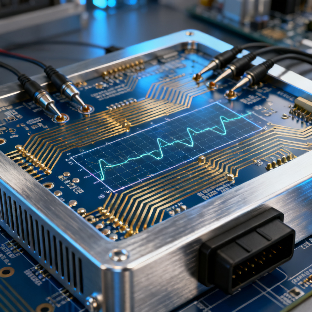
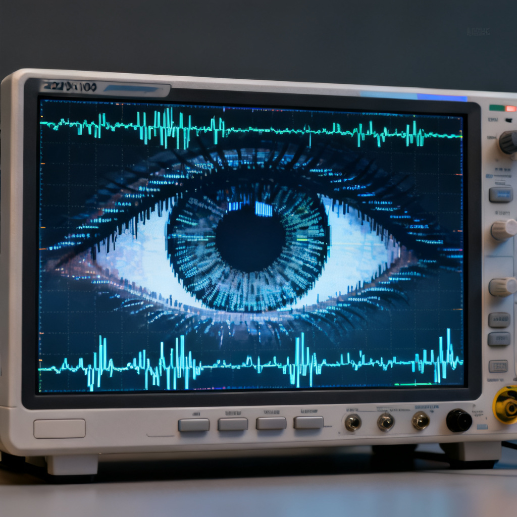
An Eye Diagram is a graphical representation formed by superimposing multiple short segments of a high-speed digital signal (such as a clock or data stream) on an oscilloscope. Its shape resembles a human eye, hence the name. The eye diagram statistically reflects signal integrity, revealing jitter, noise, crosstalk, and bandwidth limitations that traditional voltage testing cannot detect.
Test labs use an oscilloscope with sufficient bandwidth (typically 4-5 times the data rate) and a clock recovery module. The oscilloscope triggers on the data stream and samples voltage at random. After thousands of acquisitions, the “eye” opens, showing the region where the signal is stable (the eye opening) and the blurred region where transitions occur (the crossing point).
How to Read an Eye Diagram Report: Key Metrics – In-Depth Analysis of the Eye Diagram PCB Report
A professional Eye Diagram PCB Report contains several key parameters. Here is a breakdown of each:
Eye Opening (Height and Width)
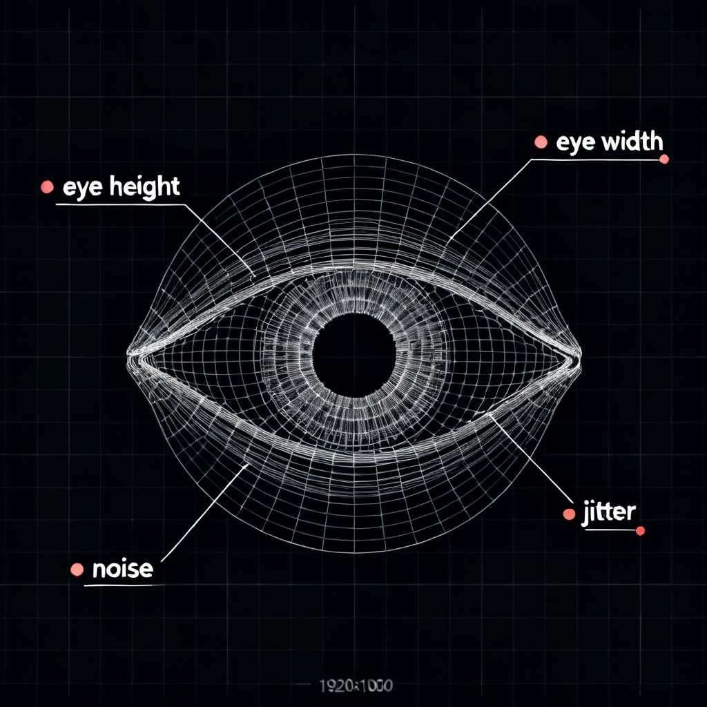
Eye Height: The voltage difference between logic “1” and logic “0” at the center of the eye diagram. Larger eye height means greater noise margin. It should typically be greater than 80% of the ideal swing.
Eye Width: The time interval over which the signal is stable. Larger eye width means greater timing margin. It should typically be greater than 60% of the unit interval.
Jitter (Timing Jitter)
Jitter is the deviation of a signal’s edge from its ideal position and is the primary cause of horizontal eye closure. Reports typically divide jitter into:
Random Jitter (RJ): Caused by thermal noise, etc., follows a Gaussian distribution, cannot be eliminated.
Deterministic Jitter (DJ): Caused by intersymbol interference (ISI), power supply noise, etc., can be further decomposed.
Total Jitter (TJ): The combination of RJ and DJ at a specific bit error rate (BER), the most important metric for compliance.
Noise (Voltage Noise)
Noise appears as vertical blurring in the eye diagram. Key metrics include:
Rise/Fall Time: The time for the signal to transition between 10% and 90%. Slow times indicate limited bandwidth.
Overshoot/Undershoot: Spikes that exceed the steady-state voltage level. Excessive overshoot can damage the receiver.
Reference Voltage Noise.
Bathtub Curve (BER Contour)
Most professional reports include a bathtub curve, which plots bit error rate against sampling point. The width of the curve at a BER of 10^-12 represents the practical usable eye width. A steep, narrow bathtub curve indicates good timing margin, while a shallow, wide curve indicates insufficient margin.
Mask Test (Compliance Pass/Fail)
Test labs overlay a mask (a geometric shape) on the eye diagram, defining forbidden regions: top mask (logic “1” must not enter), bottom mask (logic “0” must not enter), and center mask (the eye center must be clear). A PASS result means the signal did not enter any mask region. A FAIL indicates a serious signal integrity problem.
How to Verify a Test Lab’s Eye Diagram Report – Checking the Accuracy of Your Eye Diagram PCB Report
Receiving the report is only the first step. You must verify its validity. Here is a step-by-step verification process:
Check Test Setup and Equipment
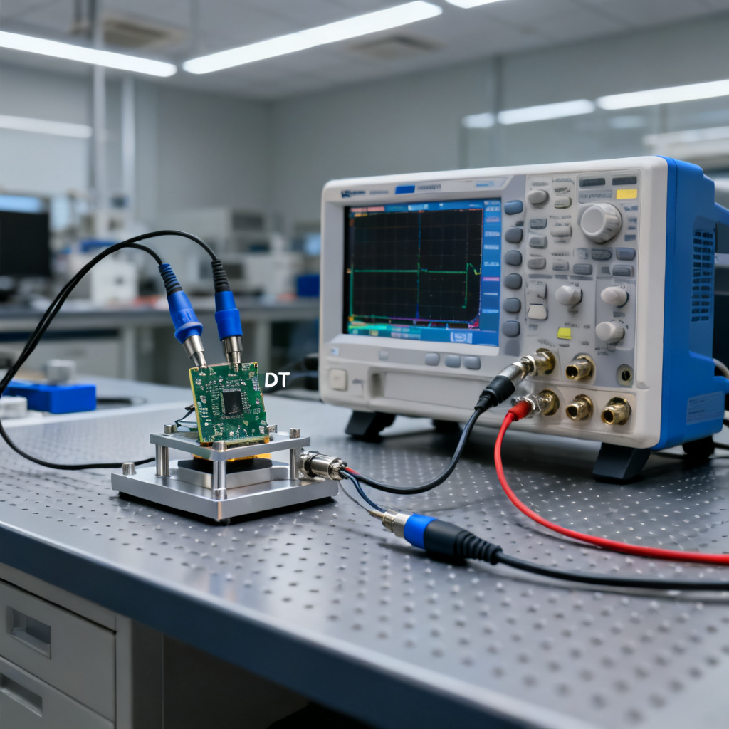
Ensure the oscilloscope bandwidth is sufficient (e.g., 20 GHz for 10 Gbps signals), low-capacitance probes (e.g., 0.3 pF) are used to avoid signal distortion, and confirm the lab calibrated the entire test path (oscilloscope + cables + probes).
Verify Pattern and Triggering
The lab should use a pseudo-random binary sequence (PRBS7, PRBS15, or PRBS31). Longer patterns (e.g., PRBS31) stress the channel more. Also, confirm the clock recovery unit (CRU) settings are correct; incorrect CRU bandwidth can lead to false jitter measurements.
Cross-Check Key Metrics
Compare the measured eye height and width with your simulation results. A 30% eye opening versus a simulated 70% suggests modeling errors or PCB fabrication issues. Ask the lab for a jitter breakdown report. High deterministic jitter points to ISI or power supply noise.
Watch for Red Flags
Overshoot > 10% typically indicates impedance mismatch or poor termination. If the eye is completely closed with extremely high jitter, the signal may be unrecoverable; request a time-domain reflectometry (TDR) measurement. If the mask test fails, find out which mask region was violated.
Request Raw Data and Repeatability Testing
Ask the lab for the raw oscilloscope data (e.g., .h5 or .mat files) so you can perform your own analysis. Also, the lab should run the test multiple times (3-5 times) to ensure consistent results.
Common Issues Revealed by Eye Diagrams and Solutions – Practical Use of the Eye Diagram PCB Report
| Eye Diagram Symptom | Root Cause | Design Fix |
|---|---|---|
| Narrow eye width, high jitter | Excessive trace length, excessive via stubs, poor impedance control | Shorten traces, use back-drilling, optimize stackup for 50Ω |
| Low eye height, high noise | Power supply noise, ground bounce, crosstalk | Add decoupling capacitors, use solid ground planes, increase trace spacing |
| Center mask failure | Severe intersymbol interference (ISI), limited bandwidth | Use low-loss dielectrics (e.g., Rogers, Megtron), reduce trace length |
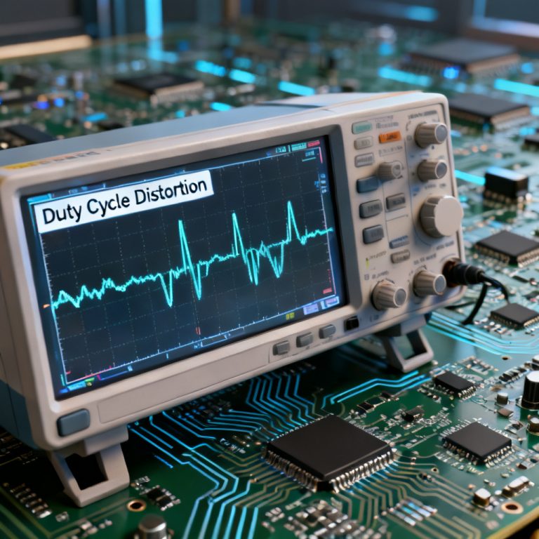
| Asymmetric eye (one edge faster than the other) | Duty cycle distortion (DCD), clock asymmetry | Check driver output, ensure differential pair routing is balanced |
| Overshoot/Undershoot | Impedance mismatch, poor termination | Add series termination resistors, optimize via geometry |
High-Speed PCB Design Best Practices: Ensuring a Clean Eye Diagram – Pre-optimization for the Eye Diagram PCB Report
To ensure your test lab report shows a clean, open eye diagram, follow these rules from the design phase:
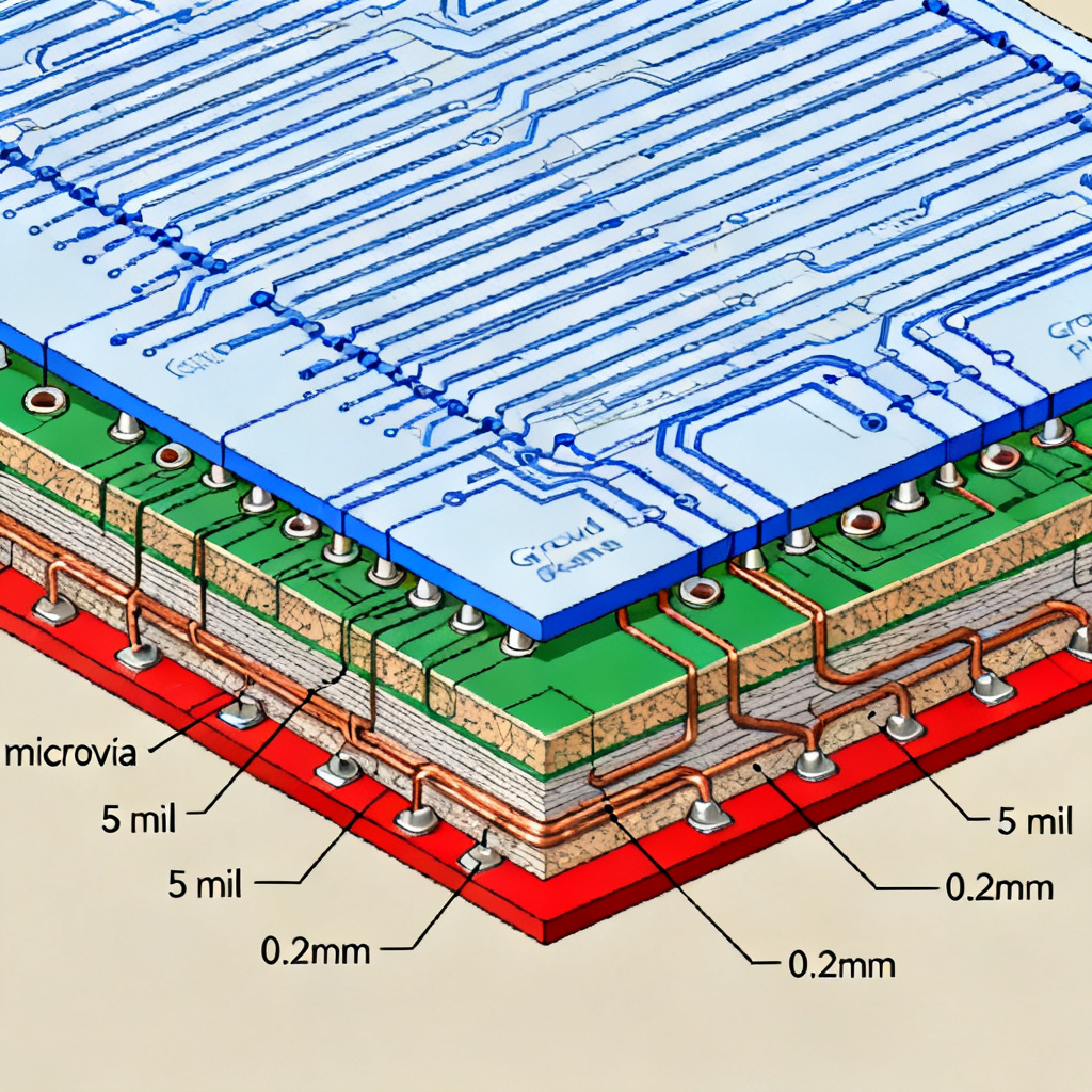
- Controlled Impedance: Maintain 50Ω single-ended / 100Ω differential impedance throughout. Use 2D field solvers to calculate trace width and spacing based on your specific stackup.
- Low-Loss Materials: For speeds above 10 Gbps, avoid standard FR-4. Use high-speed laminates like Isola 370HR, Rogers 4350B, or Megtron 6 to reduce dielectric loss and ISI.
- Via Optimization: Minimize via stubs. Use back-drilling, microvias, or buried/blind vias to eliminate unused via barrels and prevent reflections.
- Power Integrity: Power supply noise directly translates into jitter. Use solid power planes, place decoupling capacitors close to IC power pins, and use ferrite beads for isolation where needed.
- Differential Routing: Route high-speed differential pairs (e.g., USB, PCIe, Ethernet) with matched lengths and tight coupling. Avoid 90-degree corners; use 45-degree chamfers or arcs.
- Simulate Before Fabrication: Perform pre- and post-layout simulations using tools like HyperLynx, ADS, or Ansys SIwave. This can catch 90% of issues before the report.