differential pair routing is the most critical technique for reliable high-speed PCB design. This professional pillar article covers core principles, golden rules, 90Ω/100Ω impedance control, length matching standards, practical routing skills, common mistakes, protocol-specific design requirements, and mass-production DFM guidelines trusted by global industrial engineers and procurement teams.
Table of Contents
What is a Differential Pair?
Why Use Differential Pairs in High-Speed PCB Design?
The Three Golden Rules of Differential Pair Routing
Differential Impedance Control: Standard Values & Influencing Factors
Practical Field-Tested Differential Pair Routing Rules
Common Differential Pair Routing Mistakes & Correct Solutions
Serpentine Routing Design Tips for Accurate Length Matching
Differential Pair Requirements by Industry Protocol (Cheat Sheet)
Core Key Takeaways for High-Speed Differential Design
Professional PCB Design Support & Custom Service Inquiry
What is a Differential Pair?
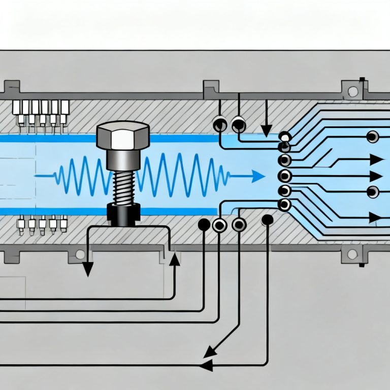
A differential pair consists of two precisely matched transmission lines with equal length, consistent trace width, fixed and continuous spacing, and complementary signal transmission modes. Unlike single-ended signals that rely entirely on the ground plane as a reference, differential pairs transmit two synchronized 180° out-of-phase signals that reference each other.
This unique structure provides inherent common-mode noise suppression. When external interference is coupled into the circuit, it affects both traces equally and is automatically offset at the receiver end, ensuring stable signal transmission in harsh industrial environments.
For more systematic high-speed design knowledge, visit our core category page: Signal Integrity.
Why Use Differential Pairs in High-Speed PCB Design?
With the rapid increase in data transmission rates, single-ended signaling can no longer meet the requirements of anti-interference, low EMI, and signal stability. differential pair routing has become the universal standard for all high-speed communication interfaces.
Core Advantages of Differential Pairs
1. Excellent Common-Mode Noise Immunity
Differential receivers only detect voltage differences and automatically filter out common-mode noise, ensuring stable transmission in complex electromagnetic environments.
2. Low EMI Radiation & EMC Compliance
The reverse electric fields between differential traces cancel each other, greatly reducing high-frequency radiation and simplifying EMC certification.
3. Higher Signal-to-Noise Ratio
Complementary differential signals double the effective voltage swing, improving anti-attenuation and long-distance transmission performance.
4. Reduced Dependence on Complete Ground Planes
Differential signals rely on mutual coupling rather than a single reference plane, adapting to complex multilayer stack-up designs.
The Three Golden Rules of differential pair routing
All professional differential designs follow three golden rules verified by Altium, Cadence, and mass-production PCB manufacturers. Strictly following these rules eliminates more than 80% of signal integrity issues.
Rule 1: Strict Intra-Pair Length Matching
Length mismatch causes timing skew, common-mode noise, EMI, and eye diagram degradation. Higher data rates require stricter matching accuracy.
| Data Rate | Maximum Length Mismatch | Control Level |
|---|---|---|
| Below 1 Gbps | 10–20 mil | Loose |
| 1–5 Gbps | 5–10 mil | Standard |
| 5–10 Gbps | 3–5 mil | Strict |
| 10–25 Gbps | 2–3 mil | Very Strict |
| 25–56 Gbps | 1–2 mil | Extreme |
| 112G PAM4 | Less than 1 mil | Limit Precision |
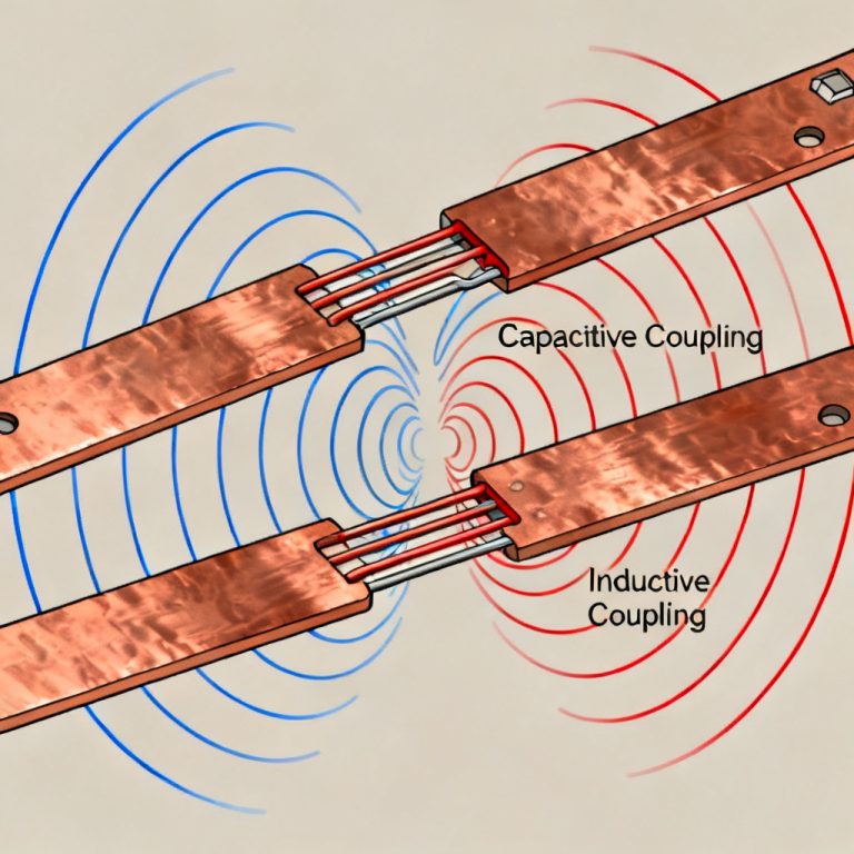
Rule 2: Constant Gap & Continuous Spacing
Any sudden change in trace spacing will cause impedance discontinuity, signal reflection, and waveform distortion. The gap must remain fixed from the driver pin to the receiver pin.
Rule 3: Tight Electromagnetic Coupling
Tight coupling maximizes noise immunity and impedance stability. The recommended ratio is S ≤ 1W for all high-speed interfaces.
| Coupling Type | S/W Ratio | Application |
|---|---|---|
| Tight Coupling | S ≤ 1W | High-speed interfaces (PCIe, USB, HDMI) |
| Medium Coupling | 1–2W | Medium-rate signals |
| Loose Coupling | S > 2W | Not recommended for high-speed design |
Differential Impedance Control
Accurate impedance matching is the core premise of stable high-speed signal transmission. Mismatched impedance leads to signal reflection, resonance, and link failure.
| Differential Impedance | Applicable Protocols | Allowable Tolerance |
|---|---|---|
| 90Ω | USB 2.0, USB 3.2, USB4 | ±10% |
| 100Ω | PCIe 4.0/5.0, HDMI 2.1, Ethernet, LVDS | ±10% |
| 85Ω | Some DDR5 interfaces | ±10% |
Simplified impedance formula: Zdiff ≈ 2 × Z0 × (1 – k)
Key influencing factors: trace width, trace spacing, dielectric thickness, and dielectric constant (Dk).
Practical differential pair routing Rules
1. Maintain Complete Symmetry
All bends, obstacles, and layer transitions must be synchronized for both traces to avoid imbalance and skew.
2. Use Paired Symmetric Vias
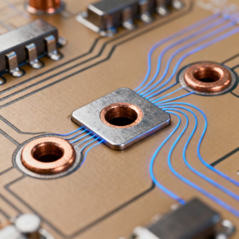
Differential vias must be placed in pairs with consistent size and spacing. Add ground vias nearby to optimize return paths.
3. Prohibit 90° Right-Angle Bends
Use 45° or arc corners to avoid impedance discontinuity and signal reflection.
4. Synchronous Layer Transition
Both traces must switch layers at the same position. Always add ground stitching vias at layer transition points.
5. Maintain Isolation Spacing
– ≥ 3W from ordinary single-ended signals
– ≥ 4W from other differential pairs
– ≥ 5W from high-speed clock signals
Common Mistakes & Correct Solutions
| Common Mistakes | Consequences | Correct Solution |
|---|---|---|
| Uncontrolled length skew | Common-mode noise, EMI, poor eye diagram | Precise serpentine length compensation |
| Inconsistent trace spacing | Impedance fluctuation, signal reflection | Fixed spacing throughout the path |
| Crossing split ground planes | Broken return path, strong radiation | Route over solid continuous ground planes |
| Asymmetric vias | Differential imbalance, link instability | Symmetric paired vias with uniform spacing |
| Layer transition without ground vias | EMI over-limit, EMC failure | Add ground vias at all layer transition points |
Serpentine Routing for Length Matching
Serpentine routing is the most widely used method for length compensation in differential pair routing. Improper serpentine design causes secondary crosstalk and impedance issues.
| Parameter | Recommended Value |
|---|---|
| Serpentine Depth | ≤ 3 × trace width |
| Segment Spacing | ≥ 4 × trace width |
| Bend Style | Multiple small compensations |
Protocol Requirements Cheat Sheet
Different high-speed protocols have specific differential design thresholds. This Table supports rapid design confirmation.
| Protocol | Differential Impedance | Max Skew |
|---|---|---|
| USB 2.0 | 90Ω | 20 mil |
| USB 3.2 | 90Ω | 5 mil |
| USB4 | 90Ω | 2 mil |
| PCIe 4.0 | 100Ω | 5 mil |
| PCIe 5.0 | 100Ω | 2–3 mil |
| HDMI 2.1 | 100Ω | 5 mil |
| LVDS | 100Ω | 10 mil |
| 100G Ethernet | 100Ω | 3 mil |
Core Key Takeaways
1. The three core pillars of qualified differential pair routing are length matching, constant spacing, and tight coupling.
2. Higher data rates require ultra-precise length control.
3. Standard 90Ω and 100Ω impedance must be controlled within ±10% tolerance.
4. Symmetric routing, paired vias, 45° corners, and ground vias are mandatory design specifications.
5. Always follow protocol-specific parameters to ensure design compliance and mass-production stability.
Professional PCB Design Support & Custom Service Inquiry
High-speed differential pair routing involves stack-up design, impedance simulation, signal integrity analysis, and DFM manufacturability verification. Professional guidance can significantly reduce prototype iterations, shorten development cycles, and lower overall costs.
Our expert engineering team provides global industrial buyers and engineers with one-stop high-speed PCB solutions:
✅ Free differential pair design review
✅ Accurate impedance calculation and stack-up suggestions
✅ Professional PCIe, USB, HDMI, Ethernet design support
✅ Mass production DFM optimization and yield improvement
✅ Customized quotation and technical consultation
If you need professional support for your high-speed PCB project, feel free to contact us for a free design assessment and personalized quote. We deliver fast response and reliable industrial-grade solutions for your mass-production projects.
Return to our signal integrity resource center: Signal Integrity.