Automating return path PCB design validation using Python scripts is essential for high-speed PCB integrity. Manual validation of return paths is tedious, error-prone, and often incomplete, especially as board complexity increases. Automating this validation with Python scripts not only saves time but ensures consistent, repeatable analysis across every design revision.
This comprehensive guide combines proven methodologies from leading PCB design authorities, covering the core concepts of return path physics, the structure of a Python-based validation script, and practical implementation steps for your design flow.
1. Understanding Return Path Physics for PCB Design Validation
Before writing a single line of Python for return path PCB design validation, you must understand what constitutes a valid or invalid return path. The key principle is that high-frequency signals always return via the path of least impedance, not least resistance. This path is directly under the signal trace, on the adjacent reference plane.
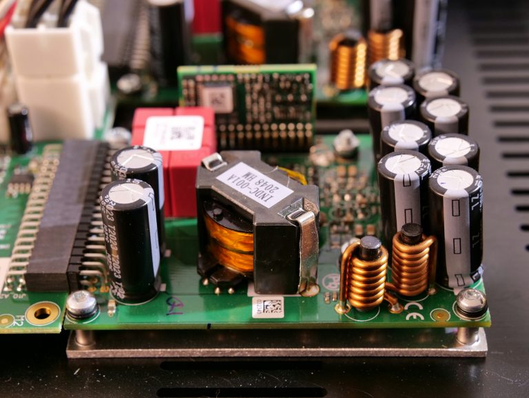
1.1 The Critical Role of the Reference Plane in High-Speed PCB
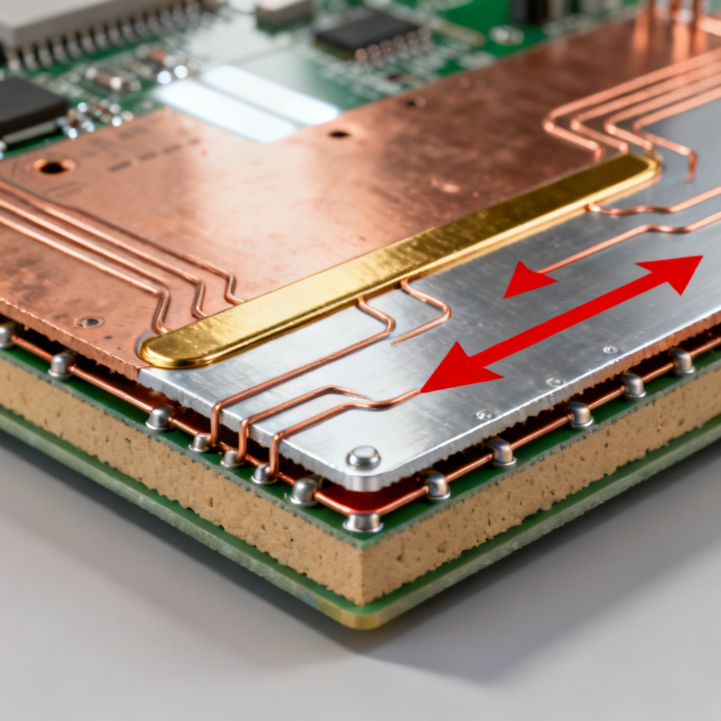
For a microstrip trace on the top layer, the ideal return path is on the ground plane directly beneath it. If this plane is continuous, the return current flows in a narrow band (approximately 3–5 times the dielectric height) under the trace, minimizing loop area and inductance.
Problems arise when:
- The reference plane is split (e.g., analog and digital ground splits).
- The signal transitions between layers (via stitching is missing or poorly placed).
- The plane has cutouts or voids (e.g., anti-pads, mounting holes, or routing channels).
- The return path is forced to detour around obstacles, increasing loop area.
1.2 Signal Layer Transitions and Via Stitching for Return Path PCB Design Validation
When a signal moves from Layer 1 to Layer 3, its return current must also switch reference planes. If the return via (a ground via placed adjacent to the signal via) is absent or too far away, the return current must find an alternative path through the board’s power distribution network (PDN), creating a large current loop. This is a primary source of radiated emissions.
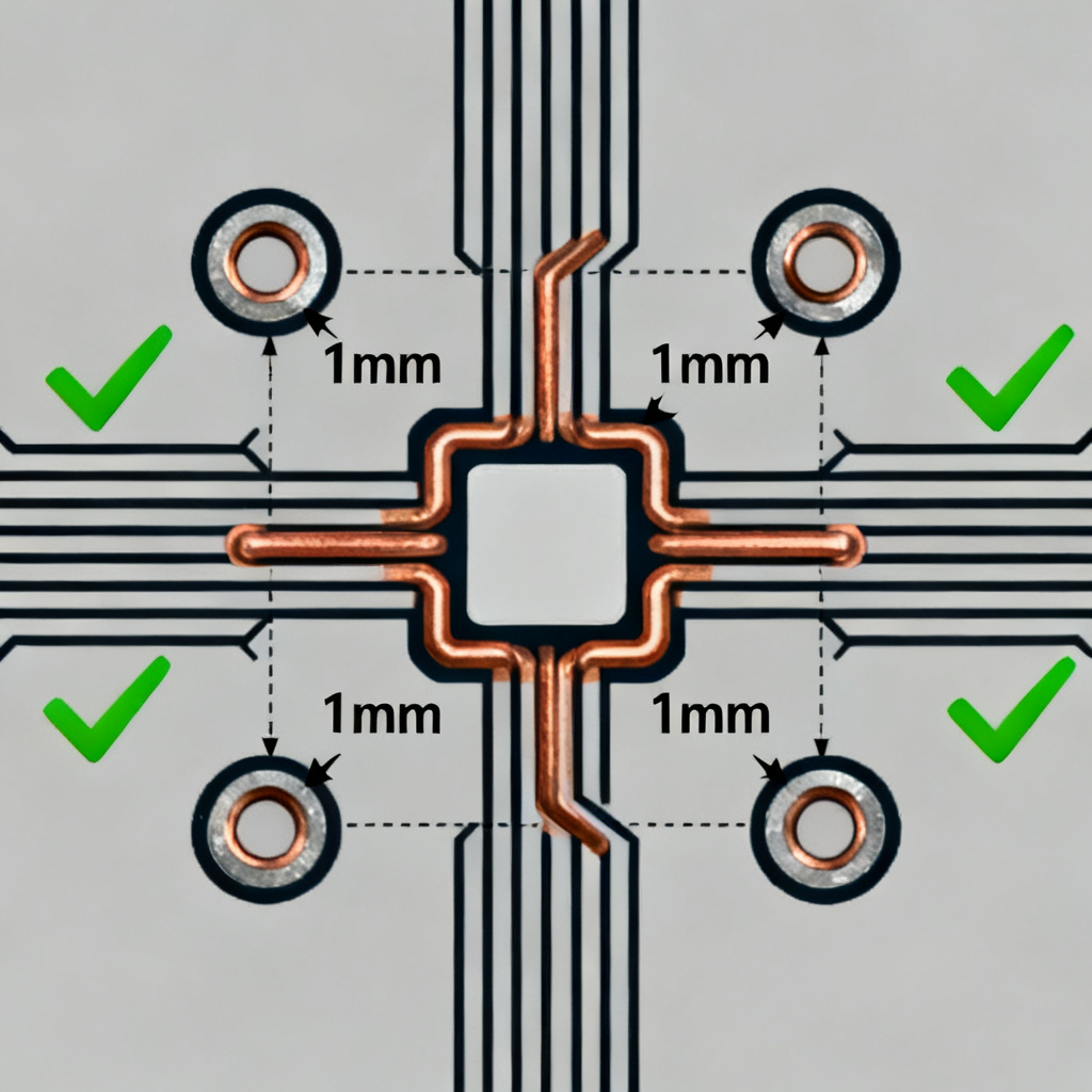
Rule of thumb: For every signal via, place a ground via within 1 mm (40 mils) to maintain a low-impedance return path.
1.3 Plane Splits and Cutouts in High-Speed PCB
A split in the ground plane acts as a barrier. If a high-speed trace crosses a split, the return current must go around the split’s edge, drastically increasing loop area and inductance. This can cause signal reflections, crosstalk, and EMI.
The Python script must detect:
- Any high-speed trace that crosses a plane split.
- Any trace that passes over a large void (e.g., an oversized antipad or a keepout area).
- Any trace whose reference plane changes without a corresponding return via.
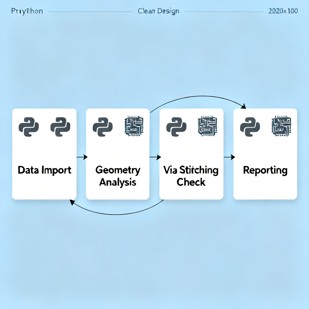
2. Building the Python Validation Script for Return Path PCB Design Validation
A robust Python script for return path PCB design validation typically consists of four functional modules: data import, geometry analysis, via stitching check, and reporting.
2.1 Data Import and Preprocessing for Return Path PCB Design Validation
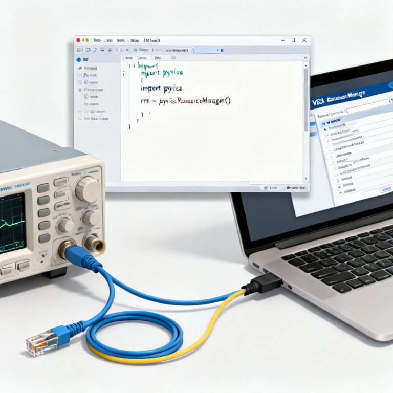
The script must read the PCB layout data. The most common format for this is ODB++ or Gerber files, but IPC-2581 or Altium’s ASCII export are also viable. For maximum flexibility, use the pcb-tools library (for Gerber) or pyodb (for ODB++).
Key data structures to extract:
- Net list: Signal names, pin locations, via locations.
- Layer stackup: Material, thickness, copper weight, plane layers.
- Plane polygons: Ground and power plane shapes (with voids).
- Trace segments: Start/end points, width, layer.
# Example: Extract trace segments from ODB++ using pyodb
import pyodb

board = pyodb.parse_design("design.odb")
signal_net = board.get_net("USB_D+")
trace_segments = signal_net.get_traces(layer="TOP")
2.2 Geometry Analysis: Trace-to-Plane Proximity for Return Path PCB Design Validation
This module checks whether a trace’s entire length has a continuous reference plane directly beneath it.
Algorithm:
- For each trace segment, sample points along its path (e.g., every 0.5 mm).
- At each sample point, project vertically down to the nearest reference plane layer.
- Check if the projected point lies inside the plane polygon (excluding voids).
- If the point falls into a void or outside the plane, flag a violation.
Handling splits: If the trace crosses a boundary between two plane polygons (e.g., two ground pours with a gap), the script should detect the gap and flag it.
def check_reference_plane(trace_point, plane_polygon, voids):
    point = (trace_point.x, trace_point.y, trace_point.z)
    if not point_in_polygon(point, plane_polygon):
        return False  # Outside plane
    for void in voids:
        if point_in_polygon(point, void):
            return False  # Inside void
    return True
2.3 Via Stitching Verification for Return Path PCB Design Validation
This module ensures that every signal via that changes layers has a corresponding return via (ground via) within a defined distance.
Algorithm:
- For every signal via, identify its layer transition (e.g., from Layer 2 to Layer 4).
- Find all ground vias within a radius (e.g., 1 mm) of the signal via.
- If no ground via is found, flag a violation.
- Additionally, check that the ground via is connected to the correct reference plane on both layers.
Consideration for power planes: If the signal transitions from a ground plane to a power plane, the return via must connect to both planes (e.g., a capacitor stitching via).
def check_via_stitching(signal_via, ground_vias, max_distance=1.0):
    for gnd_via in ground_vias:
        distance = euclidean_distance(signal_via, gnd_via)
        if distance <= max_distance:
            return True
    return False
2.4 Reporting and Visualization for Return Path PCB Design Validation
The script should generate a clear, actionable report. A good report includes:
- Summary: Total violations, criticality level (e.g., high/medium/low).
- List of violations: Net name, layer, coordinates, type (split crossing, missing return via, plane void).
- Visualization: A top-down view of the board with violations highlighted (e.g., red circles for missing vias, yellow lines for split crossings).
Use matplotlib or plotly for visualization. Export the report as HTML or PDF for easy sharing.
# Example: Generate violation markers on a board plot
import matplotlib.pyplot as plt

fig, ax = plt.subplots()
plot_board_outline(ax, board)
for violation in violations:
    ax.scatter(violation.x, violation.y, c='red', s=50, label=violation.type)
plt.savefig("return_path_violations.png")
3. Practical Implementation: Step-by-Step Workflow for Return Path PCB Design Validation
Integrating the Python script into your existing PCB design flow requires careful planning. Here is a recommended workflow.
3.1 Pre-Design Setup for Return Path PCB Design Validation
- Define a design rule database: Create a JSON or YAML file that stores your company’s return path rules, such as maximum allowed distance between signal and return vias, minimum plane continuity area, and prohibited split crossing lengths.
- Standardize layer naming: Ensure your layout tools use consistent layer names (e.g., “GND1”, “PWR1”, “SIG_TOP”) so the script can parse them automatically.
3.2 Running the Validation for Return Path PCB Design Validation
Run the script after each major design milestone:
- After placement and routing: Check for obvious plane splits and missing return vias.
- Before final sign-off: Full validation with all nets.
- After any ECO (Engineering Change Order): Re-run to catch new violations.
Sample command-line execution:
bash
python validate_return_path.py --input design.odb --rules rules.json --output report.html
3.3 Interpreting Results for Return Path PCB Design Validation
The script outputs a violation list. Prioritize fixes based on signal speed and criticality:
- High priority: Violations on clock lines, differential pairs, or high-speed serial links (e.g., PCIe, USB 3.0, HDMI).
- Medium priority: Violations on medium-speed signals (e.g., DDR memory, SPI).
- Low priority: Violations on low-speed control signals (e.g., GPIO, I2C).
Example violation output:
Net: CLK_100MHz
Layer: TOP to L3
Violation: Missing return via at (x=12.34, y=56.78)
Distance to nearest GND via: 2.5 mm (exceeds limit of 1.0 mm)
Recommended action: Add a ground via within 1 mm of the signal via.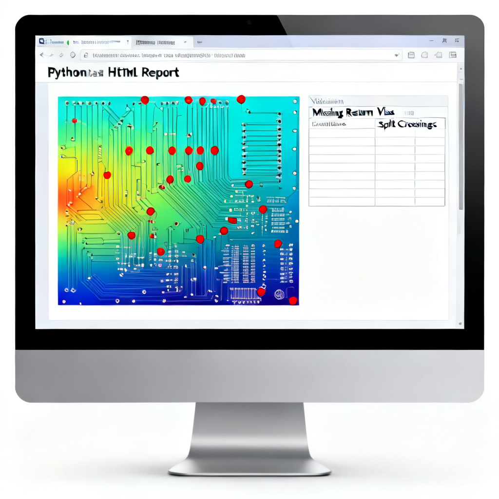
4. Advanced Considerations for High-Speed Designs in Return Path PCB Design Validation
4.1 Differential Pair Return Paths for Return Path PCB Design Validation
For differential pairs, the return path is more complex. The common-mode component still requires a continuous reference plane, but the differential-mode component is less sensitive. However, any asymmetry in the pair (e.g., length mismatch, different via distances) can convert differential-mode to common-mode, increasing EMI.
Script enhancement: For differential pairs, check that both traces have identical return path conditions (same plane, same via stitching distance). Flag any asymmetry.
4.2 Power Plane as Reference for Return Path PCB Design Validation
Sometimes a power plane (e.g., 3.3V) serves as the reference plane for a signal. In this case, the return current flows through the power plane. The script must check that the power plane is continuous and that decoupling capacitors are placed near the source and load to provide a low-impedance path back to ground.
Validation rule: For signals referenced to a power plane, verify that at least one decoupling capacitor (with appropriate value) is placed within 2 mm of the signal’s source and load pins.
4.3 Buried and Blind Vias for Return Path PCB Design Validation
High-density designs often use buried or blind vias. These can create hidden return path issues. For example, a blind via that starts on Layer 1 and ends on Layer 4 may have a missing return via on intermediate layers.
Script enhancement: For each non-through via, check that a return via (or a via with the correct net) exists on every layer the signal via touches.
5. Script Optimization and Performance for Return Path PCB Design Validation
For boards with thousands of nets and tens of thousands of trace segments, geometry checks can be slow. Use spatial indexing (e.g., R-tree via rtree library) to speed up proximity searches.
from rtree import index

# Index ground vias for fast nearest-neighbor search
idx = index.Index()
for i, via in enumerate(ground_vias):
    idx.insert(i, (via.x, via.y, via.x, via.y))

# Query nearest ground via to a signal via
nearest = list(idx.nearest((signal_via.x, signal_via.y, signal_via.x, signal_via.y), 1))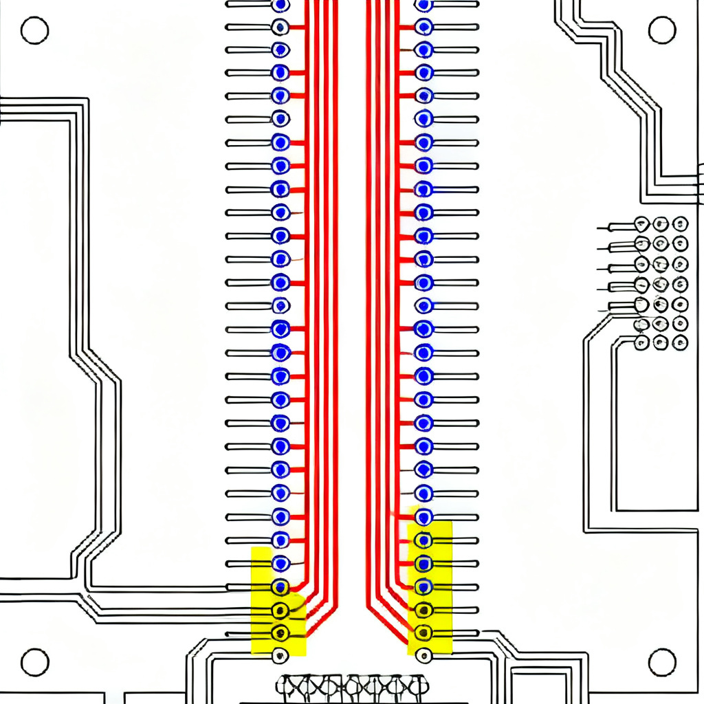
6. Comparison: Manual vs Automated Return Path PCB Design Validation
| Aspect | Manual Return Path PCB Design Validation | Automated Return Path PCB Design Validation Using Python Scripts |
|---|---|---|
| Time per board | Hours to days for complex designs | Minutes to seconds |
| Consistency | Varies with engineer experience | 100% repeatable |
| Error detection | Prone to missed violations | Systematic coverage |
| Scalability | Difficult for large boards | Handles thousands of nets |
| Reporting | Manual notes and screenshots | Automated HTML/PDF reports |
7. Key PCB Design Terminology for Return Path PCB Design Validation
- Return path: The path taken by the return current of a high-speed signal, ideally directly under the signal trace on the adjacent reference plane.
- Reference plane: A continuous copper layer (typically ground or power) that provides a low-impedance return path for signals.
- Via stitching: The practice of placing ground vias adjacent to signal vias to maintain a continuous return path during layer transitions.
- Plane split: A gap or separation in a reference plane that disrupts the return path, increasing loop inductance and EMI.
- Loop inductance: The inductance of the current loop formed by the signal trace and its return path; minimizing this is critical for high-speed signal integrity.
8. FAQ: Return Path PCB Design Validation Using Python Scripts
What is return path PCB design validation?
Return path PCB design validation is the process of verifying that every high-speed signal has a continuous, low-impedance return path, typically through an adjacent reference plane. Automated validation using Python scripts checks for plane splits, missing return vias, and other discontinuities.
Why use Python scripts for return path PCB design validation?
Python scripts automate the tedious and error-prone manual inspection of return paths, providing consistent, repeatable, and fast validation. They can handle complex, multi-layer boards with thousands of nets, ensuring high-speed signal integrity and reducing EMI risks.
How does a Python script detect return path discontinuities?
The script reads PCB layout data (e.g., ODB++), samples points along each trace, projects them onto the reference plane, and checks if they fall inside plane polygons (excluding voids). It also verifies that every signal via has a ground via within a specified distance.
What are the key benefits of return path PCB design validation automation?
Automation reduces design time from hours to minutes, eliminates human error, provides comprehensive coverage of all nets, and generates detailed reports for design review. This leads to fewer respins and higher first-pass success rates for high-speed PCBs.
Can the Python script handle differential pair return paths?
Yes, enhanced scripts check that both traces in a differential pair have identical return path conditions, including same reference plane and equal via stitching distances. Asymmetries that could cause common-mode conversion are flagged.
9. Conclusion and Next Steps for Return Path PCB Design Validation
Automating return path PCB design validation with Python scripts transforms a manual, error-prone task into a reliable, efficient process. By implementing the modules described—data import, geometry analysis, via stitching verification, and reporting—you can catch return path violations early in the design cycle, reducing costly respins and ensuring first-pass success for high-speed designs.
Recommended next steps:
- Start with a pilot project: Choose a moderately complex board (e.g., a 6-layer design with one or two high-speed nets) and run the script.
- Iterate on rules: Adjust your rule database based on real-world failures and successes.
- Integrate with CI/CD: If your design team uses version control, add the script as a pre-commit hook to validate every design change.
- Share results: Generate a dashboard (using tools like Grafana or a simple Flask app) to track violation trends across projects.
By making return path PCB design validation an automated part of your design flow, you not only improve signal integrity and reduce EMI but also empower your engineering team to focus on innovation rather than manual checks. This is a cornerstone of modern high-speed PCB design.