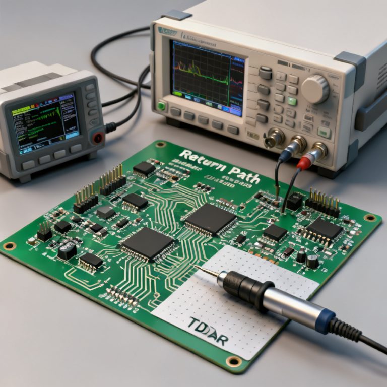
Return path PCB design report is a critical document for validating signal integrity and EMC compliance in high-speed PCB design reviews. This guide provides a step-by-step methodology to generate a comprehensive report that identifies return path violations, optimizes via placement, and ensures continuous reference planes.
1. Understanding Return Path Fundamentals for Your Report
Every return path PCB design report must start with the physics: in high-speed designs (above 100 MHz), return current flows directly under the signal trace on the adjacent reference plane. Key concepts include return current density (the 3H rule), reference plane continuity (solid planes are ideal), and via transitions (each layer change requires a nearby stitching via). Your report must document impedance of the return path, plane splits, and stitching via proximity.
1.1 Return Current Density and the 3H Rule
In a return path PCB design report, document that the majority of return current flows within a distance equal to the trace height above the plane. This is the 3H rule: if the trace height (H) above the plane is 5 mils, 90% of return current flows within 15 mils of the trace.
1.2 Reference Plane Continuity
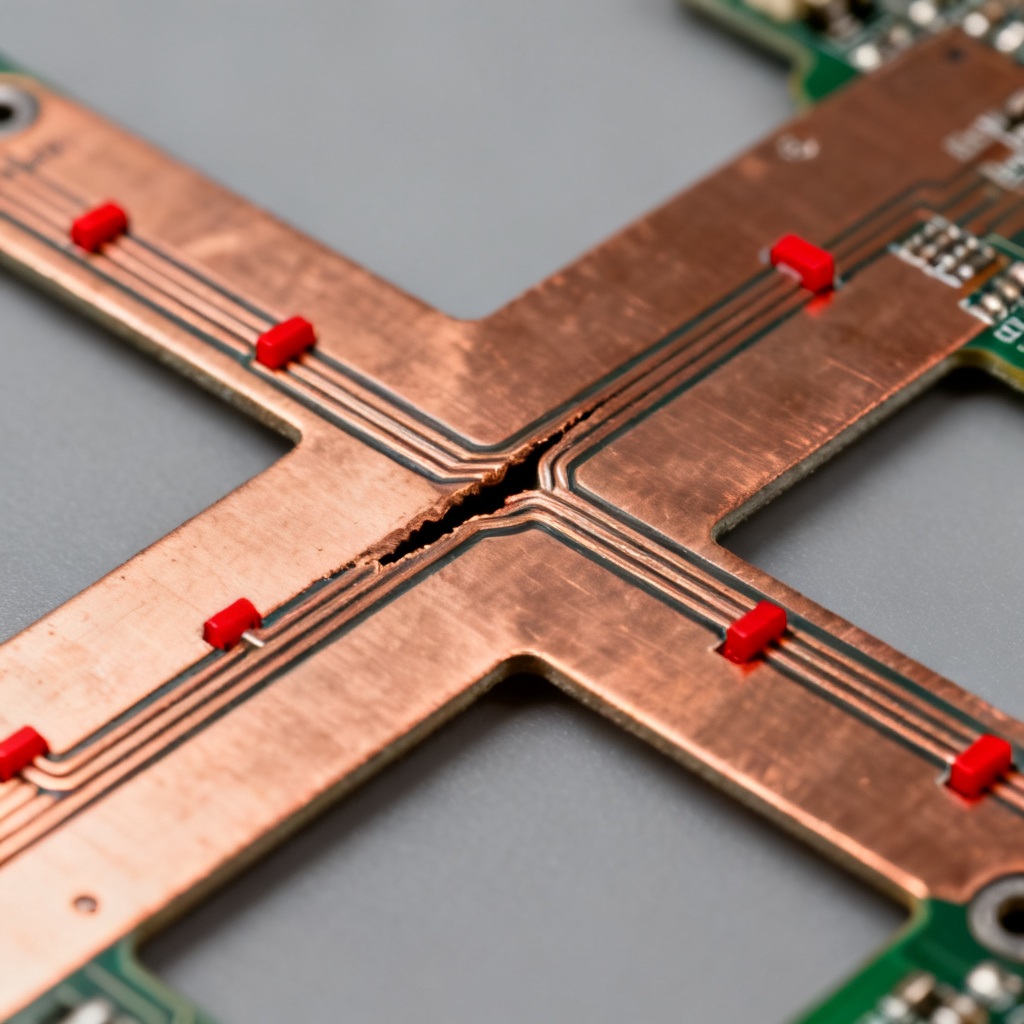
A return path PCB design report must flag any slots, splits, or gaps in the reference plane. These discontinuities force return current to detour, increasing loop inductance and causing electromagnetic interference (EMI).
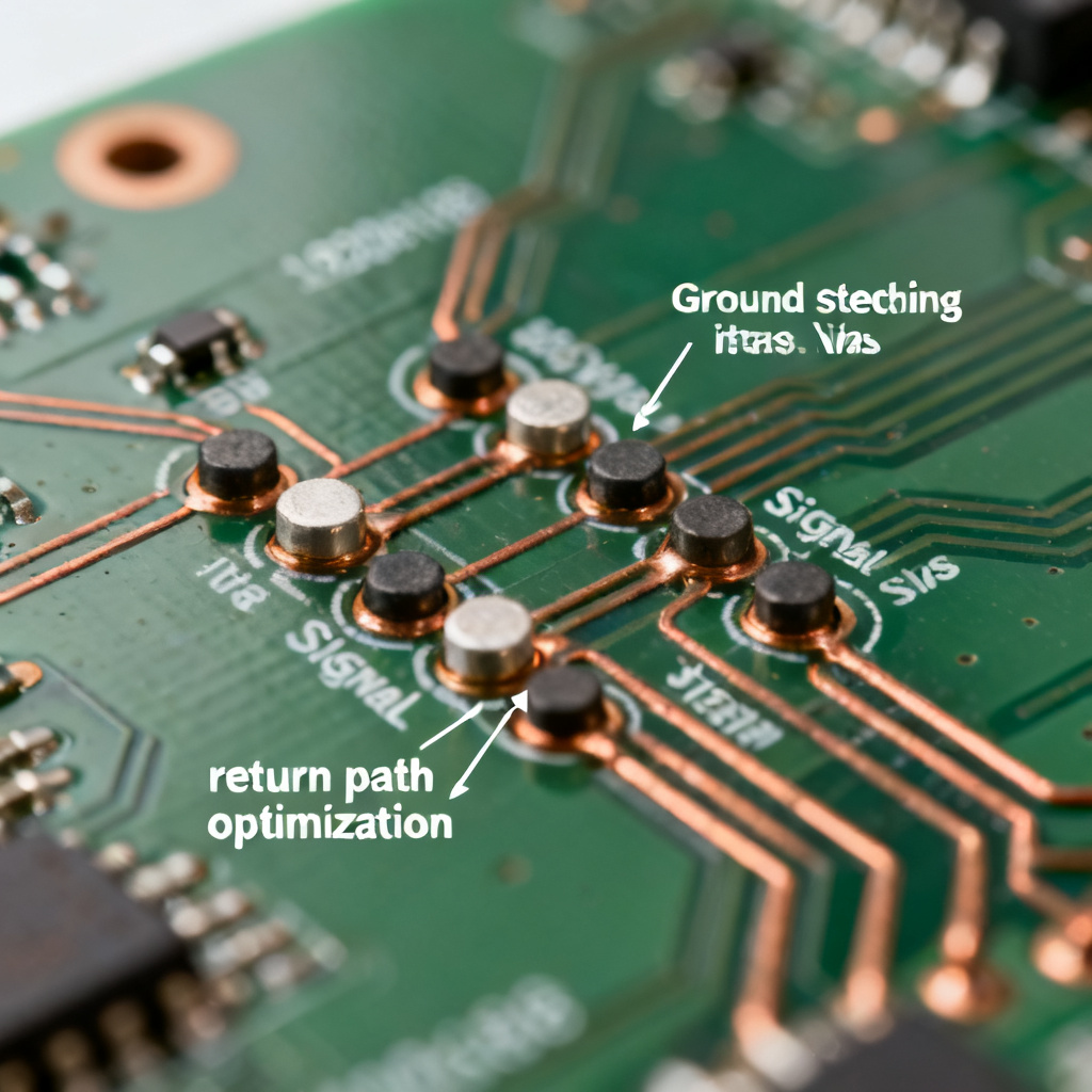
1.3 Via Transitions and Stitching Vias
When a signal changes layers, the return path PCB design report should verify that a ground stitching via is placed within 2–5 times the dielectric height (typically under 50 mils for 0.5 mm stack-up). Missing stitching vias are a top violation in high-speed designs.
2. Tools and Data for Generating a Return Path PCB Design Report
To create a return path PCB design report, you need PCB layout software (Altium Designer, Cadence Allegro, KiCad), stack-up information (layer count, dielectric thickness, copper weight, impedance targets), a signal net list identifying critical high-speed nets (DDR, PCIe, Ethernet, USB, HDMI), and optionally EMC simulation tools (HyperLynx, SIwave, Ansys Q3D).
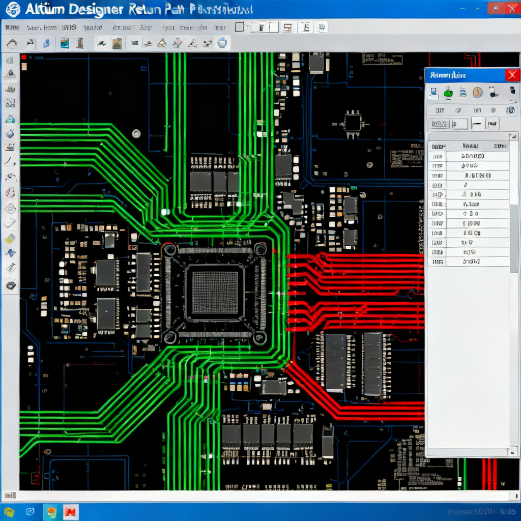
2.1 Using Altium Designer for Return Path Analysis
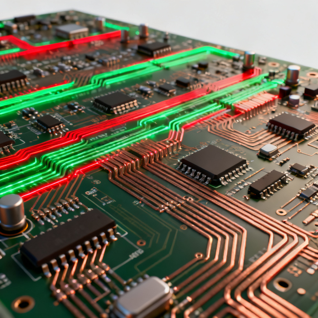
Go to Tools > Return Path Analysis, select the net(s) to analyze (e.g., DDR_DQ0), click Analyze. The tool displays the return path as a colored line (green = good, red = broken). The report tab shows path length (should be under 1.5x signal trace length), plane continuity, and via count with stitching via verification.
2.2 Using Cadence Allegro for EMI DRC
Run EMI DRC from the Analysis menu, select Return Path as the DRC type, set thresholds (max loop area, max via distance to stitching via), and generate a report in CSV or HTML format. This automates return path PCB design report generation for complex boards.
2.3 Manual Analysis in KiCad
Enable the PCB Editor with Grid and Measure tools. For each critical net, measure the distance from the signal via to the nearest GND via. Check the reference plane layer for any cutouts or slots under the trace. Manual analysis is suitable for simpler boards but error-prone for 8+ layer designs.
3. Identifying Critical Nets for Return Path Analysis
Not all signals require detailed analysis in a return path PCB design report. Prioritize high-speed differential pairs (USB 3.0, SATA, HDMI, PCIe), single-ended high-speed signals (DDR data/address/clock lines, SPI, I2C above 10 MHz), clock signals (even low frequency, fast edges cause transients), and power delivery network (PDN) paths.
3.1 Rule of Thumb for Critical Nets
Any signal with a rise time under 1 ns (frequency above 350 MHz) must have a verified return path in your return path PCB design report. For example, DDR4 signals with 200 ps rise time require immediate analysis.
3.2 Via Density Requirements
Each signal via should have a corresponding GND stitching via within 2–5 times the dielectric height. For a 0.5 mm stack-up, this is typically under 50 mils. Document this in your return path PCB design report as a key metric.
4. Running the Return Path Analysis
Follow these steps to generate a return path PCB design report using your EDA tool:
- Open the PCB document in your layout software.
- Navigate to the return path analysis feature (e.g., Altium: Tools > Return Path Analysis; Allegro: Analysis > EMI DRC).
- Select critical nets from your prioritized list.
- Run the analysis and review the output: path length, plane continuity, via count, and stitching via proximity.
- Export the report as PDF or image for inclusion in your design review presentation.
4.1 Automated Tools Are Recommended
For complex boards (8+ layers), automated tools are essential for an accurate return path PCB design report. Manual analysis is error-prone and time-consuming. Always use the built-in return path analysis features of your EDA tool.
4.2 Exporting the Report
Export your return path PCB design report as PDF or image files. Include screenshots of the return path overlay, 3D views showing plane splits and via placements, and loop area calculations if available from simulation.
5. Interpreting Results and Identifying Violations
Your return path PCB design report should highlight three main types of violations:
| Violation Type | Description | Effect | Report Entry Example |
|---|---|---|---|
| Plane Splits and Slots | Trace crosses a gap in the reference plane (e.g., between power islands) | Return current loops around the gap, increasing inductance and causing EMI | “Net CLK_100MHz crosses a 50 mil slot between VCC_3.3V and GND planes. Risk: High loop inductance.” |
| Missing Stitching Vias | Signal changes layers but no GND via near the transition | Return current takes a long path through board edge or power vias, causing crosstalk | “Via transition for net ETH_TXP at (X,Y) has no stitching via within 100 mils. Required: under 30 mils.” |
| Improper Reference Plane Assignment | Signal trace referenced to a power plane not AC-coupled to GND | Return path is not continuous at high frequencies | “Net USB_DP is referenced to VCC_5V plane. Add 0.1 µF decoupling caps near both endpoints.” |
5.1 Plane Splits and Slots
In your return path PCB design report, document each plane split with its location (X,Y coordinates), the net name, and the gap width. Recommend solutions such as moving the trace to avoid the slot or adding a bridge capacitor across the split.
5.2 Missing Stitching Vias
For each via transition without a nearby stitching via, your return path PCB design report should specify the required distance (under 30 mils) and the current distance (e.g., 100 mils). This is a high-severity violation that must be fixed before fabrication.
5.3 Improper Reference Plane Assignment
When a signal is referenced to a power plane without AC coupling, your return path PCB design report should recommend adding decoupling capacitors (0.1 µF) near both endpoints to provide an AC return path. This is a medium-severity violation.
6. Documenting the Return Path PCB Design Report
A professional return path PCB design report should include:
- Executive Summary: Board name, date, reviewer, summary of findings (e.g., “Analyzed 45 critical nets. Found 12 violations: 5 plane splits, 4 missing stitching vias, 3 improper plane references. All violations are categorized as High Risk.”)
- Detailed Violation Table: Net name, violation type, location (X,Y), severity (High/Medium/Low), recommendation
- Visuals: Screenshots of return path overlay, 3D views, loop area calculations
- Risk Matrix: Prioritize fixes by severity
- Reference to IPC-2152: Standards for plane continuity guidelines
6.1 Executive Summary
Start your return path PCB design report with an executive summary that includes the board name (e.g., “High-Speed ADC Board v2.1”), date (e.g., “2025-04-07”), reviewer (e.g., “John Doe, Senior SI Engineer”), and a summary of findings with violation count and severity.
6.2 Detailed Violation Table
Create a table in your return path PCB design report with columns for Net Name, Violation Type, Location (X,Y), Severity, and Recommendation. Use a traffic light color code (Red/Yellow/Green) for severity. Red = must fix before prototyping.
6.3 Visuals and 3D Views
Include screenshots of the return path overlay from your EDA tool, 3D views of the board showing plane splits and via placements, and loop area calculations if available. These visuals make your return path PCB design report more actionable during design review.
7. Validation with Simulation
For high-reliability designs (aerospace, medical, automotive), validate your return path PCB design report with 3D EM solvers such as Ansys SIwave (extract S-parameters and visualize current density), HyperLynx (run return path analysis with TDR to check impedance), or CST Studio Suite (model via transitions and plane coupling).
7.1 Simulation Report Contents
Include in your return path PCB design report: current density heatmap (hot spots indicate return path issues), impedance profile (any dip over 10% from target is a violation), and loop inductance values per net (target: under 1 nH per inch for high-speed).
7.2 Using Ansys SIwave
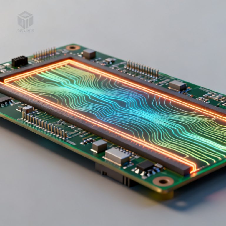
In Ansys SIwave, extract S-parameters and generate a current density heatmap. Add this to your return path PCB design report to visually show return path issues. Hot spots indicate areas where return current is forced to take a longer path.
7.3 Using HyperLynx for TDR
Run time-domain reflectometry (TDR) in HyperLynx to check impedance along the return path. Any impedance dip over 10% from target should be flagged in your return path PCB design report as a violation.
8. Presenting the Report in a Design Review
When presenting your return path PCB design report, follow this structure: Slide 1: Title and Objective (“Return Path Analysis for High-Speed ADC Board”), Slide 2: Methodology (“Used Altium Return Path Analysis tool with IPC-2152 guidelines”), Slide 3: Key Findings (violation table and heatmap), Slide 4: Critical Violations (focus on nets that could cause failure, e.g., clock, DDR), Slide 5: Action Plan (“Fix 12 violations within 2 weeks; re-run analysis”), Slide 6: Q&A.
8.1 Traffic Light Color Code
Use a traffic light color code (Red/Yellow/Green) for violation severity in your return path PCB design report. Red = must fix before prototyping, Yellow = should fix, Green = acceptable. This helps the design review team prioritize actions.
8.2 Action Plan
Include a clear action plan in your return path PCB design report: “Fix 12 violations within 2 weeks; re-run analysis; schedule follow-up review.” Assign owners for each violation to ensure accountability.

9. Common Mistakes to Avoid
Based on top sources, the most frequent errors in a return path PCB design report include:
- Ignoring power planes: Many designers only check GND planes, but power planes also carry return current if AC-coupled. Include power plane analysis in your report.
- Overlooking via antipads: Large antipads can block return current flow. Check antipad size in your return path PCB design report.
- Assuming all layers are equal: The return path is shortest on the layer adjacent to the signal. A trace on layer 1 referenced to layer 2 is fine, but if layer 2 is a split plane, the path is broken.
- Not updating the report after layout changes: Always re-run analysis after moving vias or planes. Your return path PCB design report should be a living document.
10. Best Practices and Conclusion
Generating a return path PCB design report is a systematic process that combines EDA tool analysis, manual inspection, and simulation. For high-speed designs (e.g., 1 Gbps+), this report is non-negotiable for ensuring signal integrity and passing EMC tests. Remember: always prioritize continuous GND reference planes for critical nets, place stitching vias within 2x the dielectric height of signal vias, document every violation with location, severity, and a clear fix, and use the report as a living document throughout the design cycle. By following this guide, you will produce a return path PCB design report that earns trust during design reviews, reduces prototyping iterations, and ensures your high-speed PCB performs reliably in the field.
10.1 Continuous GND Reference Planes
Always prioritize continuous GND reference planes for critical nets in your return path PCB design report. This is the single most effective way to ensure low-inductance return paths.
10.2 Stitching Via Placement
Place stitching vias within 2x the dielectric height of signal vias. Document this in your return path PCB design report as a key requirement for all via transitions.
10.3 Living Document
Use your return path PCB design report as a living document throughout the design cycle. Update it after every layout change to ensure continuous validation.
Frequently Asked Questions (FAQ)
What is a return path PCB design report?
A return path PCB design report is a structured document that visualizes and validates the return paths of signals in a high-speed PCB. It identifies violations such as plane splits, missing stitching vias, and improper reference plane assignments to ensure signal integrity and EMC compliance.
Why is return path analysis important for high-speed PCBs?
Return path analysis is critical because disrupted return paths cause signal integrity degradation, electromagnetic interference (EMI), and potential EMC test failures. A return path PCB design report helps catch these issues before fabrication.
What tools can I use to generate a return path PCB design report?
You can use Altium Designer (Return Path Analysis tool), Cadence Allegro (EMI DRC), or KiCad (manual analysis). For advanced validation, use HyperLynx, SIwave, or Ansys Q2D Extractor.
What are common violations in a return path PCB design report?
Common violations include plane splits and slots, missing stitching vias, and improper reference plane assignment. Each should be documented with location, severity, and a clear fix.
How often should I update my return path PCB design report?
Update your return path PCB design report after every layout change, including moving vias, adding traces, or modifying planes. It should be a living document used throughout the design cycle.
Return path PCB design report best practices: always prioritize continuous GND reference planes, place stitching vias within 2x dielectric height, and document every violation. Contact our engineering team for a free design review consultation. We specialize in high-speed PCB fabrication and can help optimize your design for manufacturing.